
Official websites use .gov
A .gov website belongs to an official government organization in the United States.
Secure .gov websites use HTTPS
A lock (
) or https:// means you’ve safely connected to the .gov website. Share sensitive information only on official, secure websites.
Summary
The interest in using graphene as an electronic material arises in large part from the high speed with which electrons move through the material — approximately 100 times faster than in the silicon used in almost all modern electronic devices. Graphene is a single atomic layer of carbon with the thickness of a single carbon atom, making it ideal for small electronic devices like transistors or sensors. Graphene can be patterned using standard semiconductor lithography techniques, and can serve as both the active element of the electrical component and also as the "wires" or connections to other parts of the electrical circuit. However, the properties of graphene that make it so attractive are altered when graphene contacts other materials in an electrical device. The environment that graphene is placed in can lead to ripples in the graphene's structure and electrical properties, affecting how well the charge carriers can go through the graphene circuit. Ultimately, these effects determine how well the electrical device performs. The goal of this project is to develop atomic scale measurements using the CNST's custom built scanning probe microscopes to determine how graphene's electronic properties are altered when graphene is in contact with other materials in an electrical device. These measurements will help enable the optimization of graphene electronic devices and the future commercialization of graphene-based electronic technologies.
Description
Two of the remarkable features of graphene that are opening avenues to multiple applications are its high transport carrier mobility and the broad tunability of its electronic properties. Graphene charge carriers can be tuned continuously from negative carriers (i.e., electrons), to positive (holes). Separating the point between the negative and positive carriers is a neutrality point where the charges go to zero. This condition is called the Dirac point , named after the Dirac theory used to describe graphene charge carriers. When graphene contacts other materials, like the substrates used in electronic devices, experimental measurements indicate that the carriers have difficulty going through the graphene. Contact with the other materials causes variation in carrier density, even from positive to negative charges from one location to another, leading to so-called electron or hole puddles. These puddles may be due to ripples in the graphene when is lies on the substrate, or perhaps charged impurities in the substrate material. Microscopic measurements are needed to get a view of the underlying effects of other materials in contact with graphene and how these effects change electrical transport through the graphene.
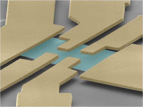
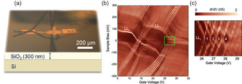
To perform measurements on graphene devices, NIST researches have to fabricate a representative electrical device. A typical semiconductor device is a complex "sandwich" of alternating conducting, semiconducting, and insulating layers and structures. To perform experiments on graphene devices, the NIST team fabricated structures with a single atomic sheet of graphene and another conductor separated by an insulating layer. When the bottom conductor is charged, it induces an equal and opposite charge in the graphene layer, and in this way the carriers can be switched from electrons (negative charges) to holes (positive charges). To determine how the graphene carriers are affected by the substrate insulators, NIST researchers used custom designed scanning probe microscopes . A unique feature of the NIST microscopes is the ability to optically align the SPM probe tip to the very small active graphene area on the device, which may be as small as tens of micrometers in length [Fig. 1(a)]. Once aligned, the microscope is cooled to liquid He temperatures (4 K) and tunneling microscopy and spectroscopy measurements are performed to probe the graphene carriers on the atomic scale.
The NIST team has developed a novel, microscopic SPM-based measurement technique, called gate mapping tunneling spectroscopy [Fig. 1(b)] to observe the nanoscale spatial variations in carrier density. In this method the tunneling conductance is measured as a function of energy at constant gate potential, and then the spectra is repeated with a small incremental change in gate potential. The resulting data is displayed in a map, showing a rich variety of detail that cannot be gathered by a single tunneling spectrum.
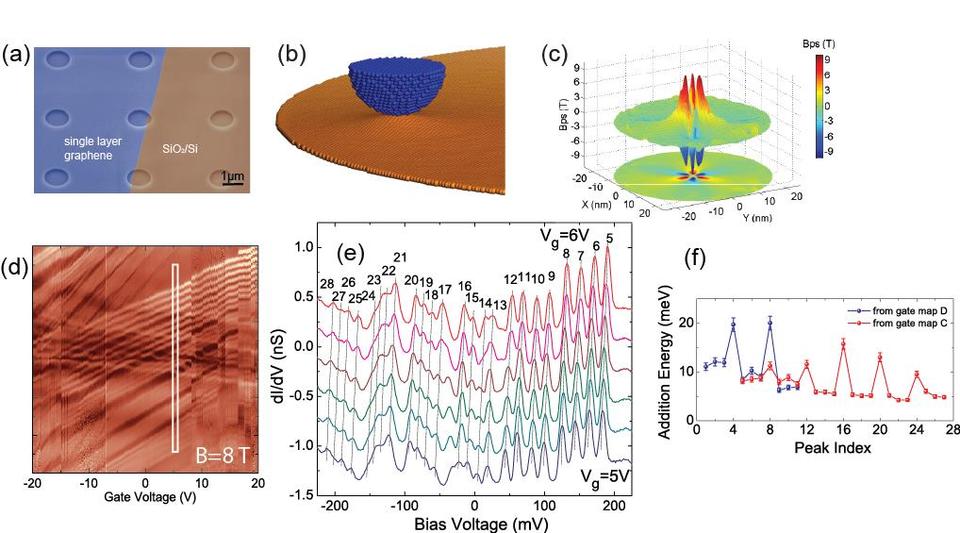
Using these methods the NIST team determined that the silicon oxide substrate potential fluctuations are interrupting the orbits of the electrons in the graphene, creating wells where the electrons and holes pool and reducing their mobility. The resulting p-n junctions (neighboring electron and hole regions) only localize the graphene carriers weakly due to the ability of graphene carriers to penetrate potential barriers. However, the NIST team found a dramatic change when a magnetic field was applied. The electrons lacked the energy to scale the barriers of resistance created by energy gaps between the Landau levels and settle into isolated pockets of graphene quantum dots, nanometer-scale regions that confine electrical charges in all directions. The Coulomb charging of the quantum dots was observed by as a diamond structure in the gate maps when the Landau levels cross the Fermi energy [Fig. 1(c)].
The NIST researchers found they could create graphene quantum dots in another way by straining the graphene sheet. If you stretch graphene, for example by making a graphene drumhead, the graphene charge carriers behave as if a fictitious magnetic field is applied [Fig. 2(c)]. To test this idea, the NIST researchers fabricated micrometer sized graphene drumheads by etching holes in silicon dioxide and placing a single sheet of graphene over the holes [Fig. 2(a)]. The team then performed gate mapping tunneling spectroscopy and found that quantum dots formed in the graphene under the probe tip because the graphene experiences extreme strain as it is attracted to the tip, much as a sheet would be strained if you were pulling on it with your fingers [Fig. 2(b)].
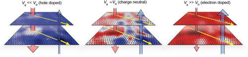
The NIST researchers found even more complicated nanoscale behavior caused by substrate interactions in bilayer graphene (two stacked graphene layers). It has been known for some time that bilayer graphene acts more like a semiconductor with a band gap when immersed in an electric field. Just like single layer graphene, the insulating substrate induces electron and hole puddles to form. However, in bilayer graphene, both electron and hole puddles are deeper on the bottom layer because the bottom layer is closer to the substrate. This difference in puddle depths between the layers creates a random pattern of alternating charges and the spatially varying band gap [Fig. 3], which was difficult to detect when the bilayer band gap was measured with macroscopic measurements.
The NIST team plans to explore further the role that substrates play in the creation and control of carrier localization and band gaps in single layer and bilayer graphene by using different substrate materials. When substrate interactions can be reduced far enough, the team expects to investigate how electrons interact on a microscopic scale, opening a path to harnessing the exotic quantum properties of bilayer graphene to create a new quantum field effect transistor.
News Articles:
NIST-led Research Group Creates First Whispering Gallery for Graphene Electrons
Real-World Graphene Devices May Have a Bumpy Ride
Two Graphene Layers May Be Better Than One
Graphene Drumheads Tuned to Make Quantum Dots
Selected Publications
- Scanning tunneling spectroscopy of proximity superconductivity in epitaxial multilayer graphene, F. D. Natterer, J. Ha, H. Baek, D. Zhang, W. G. Cullen, N. B. Zhitenev, Y. Kuk, and J. A. Stroscio, Physical Review B 93, 045406 (2016).
NIST Publication Database Journal Web Site - Strong asymmetric charge carrier dependence in inelastic electron tunneling spectroscopy of graphene phonons, F. D. Natterer, Y. Zhao, J. Wyrick, Y.-H. Chan, W.-Y. Ruan, M.-Y. Chou, K. Watanabe, T. Taniguchi, N. B. Zhitenev, and J. A. Stroscio, Physical Review Letters 114, 245502 (2015).
NIST Publication Database Journal Web Site - Programmable extreme pseudomagnetic fields in graphene by a uniaxial stretch, S. Zhu, J. A. Stroscio, and T. Li, Physical Review Letters 115, 245501 (2015).
NIST Publication Database Journal Web Site - Creating and probing electron whispering-gallery modes in graphene, Y. Zhao, J. Wyrick, F. D. Natterer, J. F. Rodriguez-Nieva, C. Lewandowski, K. Watanabe, T. Taniguchi, L. S. Levitov, N. B. Zhitenev, and J. A. Stroscio, Science 348, 672–675 (2015).
NIST Publication Database Journal Web Site - Renormalization of the graphene dispersion velocity determined from scanning tunneling spectroscopy, J. Chae, S. Jung, A. F. Young, C. R. Dean, L. Wang, Y. Gao, K. Watanabe, T. Taniguchi, J. Hone, K. L. Shepard, P. Kim, N. B. Zhitenev, and J. A. Stroscio, Physical Review Letters 109, 116802 (2012).
NIST Publication Database Journal Web Site - Electromechanical properties of graphene drumheads, N. N. Klimov, S. Jung, S. Zhu, T. Li, C. A. Wright, S. D. Solares, D. B. Newell, N. B. Zhitenev, and J. A. Stroscio, Science 336, 1557–1561 (2012).
NIST Publication Database Journal Web Site - Enhanced carrier transport along edges of graphene devices, J. Chae, S. Jung, S. Woo, H. Baek, J. Ha, Y. J. Song, Y.-W. Son, N. B. Zhitenev, J. A. Stroscio, and Y. Kuk, Nano Letters 12, 1839-1844 (2012).
NIST Publication Database Journal Web Site - Microscope polarization in bilayer graphene, G. M. Rutter, S. Jung, N. N. Klimov, D. B. Newell, N. B. Zhitenev, and J. A. Stroscio, Nature Physics 7, 649-655 (2011).
NIST Publication Database Journal Web Site - Evolution of microscopic localization in graphene in a magnetic field from scattering resonances to quantum dots, S. Jung, G. M. Rutter, N. N. Klimov, D. B. Newell, I. Calizo, A. R. Hight-Walker, N. B. Zhitenev, and J. A. Stroscio, Nature Physics 7, 245-251 (2011).
NIST Publication Database Journal Web Site