Summary
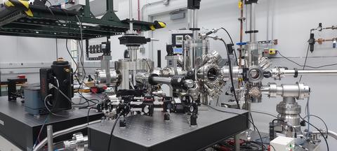
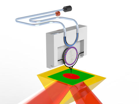
Our goal is to advance nanoelectronic/quantum materials and devices by developing the nanoscale spectroscopic metrology to measure thermal, optical, compositional, and electrical properties quantitatively with nanoscale spatial resolution.
Description

Semiconductor technologies are critical to U.S. economic and national security as they are essential to modern life in communications, healthcare, energy, etc. and also underpin many emerging technologies like quantum, artificial intelligence, high power electronics and advanced wireless (6G+). The next wave of microelectronics innovation will likely stem from the successful integration of heterogeneous materials and devices through advanced packaging enabling improved yields, functionalities, energy efficiency and cost, at the expense of increased complexity.
Novel, non-destructive, versatile metrology is needed for measuring physical properties (thermal, electrical, optical, …) defects and impurities of new materials (2D, quantum, wide bandgap) and devices with unprecedented spatial and depth resolutions, precision, sensitivity, bandwidth, and throughput is critical to accelerate R&D.

Therefore, this program will advance nanoscale resolution spectroscopic techniques to probe fundamental light-matter and electron-correlation effects at length scales relevant to emerging nanolectronics and quantum devices (typically, 1 to 1000 nm). Such new spectroscopic nanometrology will be leveraged to measure physical properties (e.g., compositional, electrical, thermal, mechanical, optical), transient carrier phenomena (e.g., excitons; polarons; trapping), and their dynamical properties (e.g., free carrier mobilities, heat diffusion) that ultimately affect device performance and efficiencies.
By opening new nanoscale and atomic scale windows for the observation of the complex phenomena mediated by correlated electrons we envision of a broad impact across emerging 2D, nanoscale and quantum materials which may lead to the discovery of new effects and to the engineering of quantum devices.

