
Official websites use .gov
A .gov website belongs to an official government organization in the United States.
Secure .gov websites use HTTPS
A lock (
) or https:// means you’ve safely connected to the .gov website. Share sensitive information only on official, secure websites.
Summary
Renewable energy sources such as solar energy are attractive alternatives to fossil fuels because of their abundant supply and pollution-free power generation. Currently, only a fraction of the energy supply for the United States comes from renewable sources, because of the high cost of materials used and their low conversion efficiency. Modern nanofabrication techniques may enable progress in this area by opening up a wider range of device architectures. The goal of this project is to develop a range of modeling and theoretical techniques to understand how modifying internal nanoscale structures whose feature sizes approach the natural length scale of important physical phenomena (e.g. the depletion width or the diffusion length) affects the performance of charge carrying devices such as solar cells and electrochemical batteries.
Description

Nanostructured materials offer potential benefits for a range of renewable energy applications that rely critically on interfaces for separating charges, including photovoltaics, thermoelectrics, and electrochemical energy storage. The use of nanostructures allows scientists and engineers to increase the chemically active surface area for any given volume in electrochemical systems, leading to higher energy and power densities. For photovoltaics, increasing the surface area between n- and p- type materials allows photoexcited charges to traverse a smaller distance before reaching the internal electric fields which separate and collect charges. This improvement makes it possible to collect photo-excited charges even in the presence of many impurities, enabling the use significantly less expensive materials.
While thermoelectrics do not rely directly on interfaces for their operation, the presence of interfaces can enhance thermoelectric efficiency by scattering heat-carrying phonons so that temperature gradients aren't shorted out by thermal currents. By acting as energy-dependent electron scatterers, interfaces also block slow ("cold") electrons and transmit fast ("hot") electrons. This energy filtering enhances the thermoelectric effect and increases the overall efficiency.
When the features in nanostructure-enabled devices approaches the length scales of the underlying physical processes, well established models, such as the planar p-n junction, no longer provide relevant guidance for system design or for the interpretation of experimental results. These new systems require modeling and theoretical analysis that realistically describes the nanostructure. We use a multi-scale approach which describes both microscopic processes utilizing first-principles calculations and device performance at a systems level by employing physics-based phenomenological models, including coupled drift-diffusion and Poisson equations. The effect of the nanostructures is incorporated into these models either explicitly through model geometry (usually for well ordered systems), or through approximations such as effective medium theory (for disordered systems).
An example of a photovoltaic with ordered nanostructures is provided by the radial silicon p-n junction array. Silicon is abundant, and its band gap is nearly optimal for solar energy conversion. However it absorbs light very poorly. Therefore, silicon solar cells must be very thick to capture all of the light. As the solar cells absorb light (photons), electrons in the material transition to a higher energy state. These electrons must traverse the large distance to the collecting electrode without decaying back to their initial state, a process known as recombination. Since impurities promote recombination, photovoltaic materials must be very pure. These requirements lead to high energy and price costs for solar grade silicon.
Nanostructure can circumvent this challenge by making the direction of light absorption orthogonal to the direction of charge collection. The radial p-n junction array (see Fig.1) has the required thickness to absorb light, but by placing p-n junctions throughout the volume of the material, the distance required to reach a charge collecting electric field and electrode is greatly reduced. This enables the use of significantly cheaper metallurgical grade silicon, reducing the cost substantially while retaining the efficiency. By modeling this system at the nanoscale, we find the optimal distance between adjacent p-n junctions to be around twice the diffusion length, and our analysis conforms well with the experimental data.
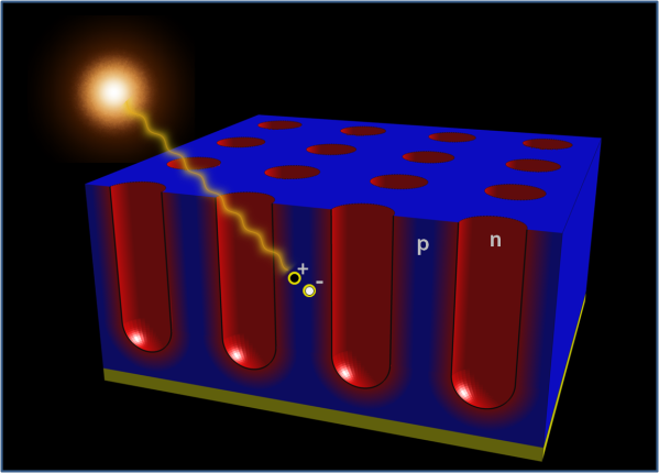
Fig. 1. A radial p-n junction array in which the direction of light collection is orthogonal to the direction of charge collection.
Other examples of the potential benefit of nanostructures are found in next-generation materials for solar cells such as cadmium telluride and copper indium gallium diselenide. These materials absorb light much more effectively than silicon and therefore require a much thinner active layer. In both cases, the materials are polycrystalline, with grain boundaries separating volumes with different crystal orientations. Usually grain boundaries are recombination centers, and are therefore detrimental to device performance. However, in these materials grain boundaries inhibit recombination for reasons that are not fully understood. We use a first-principles approach to understand how the atomic structure of defects affects the electronic structure in such a way as to inhibit recombination. These microscopic models give insight into the origin of the phenomenological parameters used in the drift-diffusion level of description. Combining the two approaches allows multi-scale modeling that connects microscopic processes to overall device performance.
Thermoelectrics present challenges due to conflicting materials requirements. A good thermoelectric has a low thermal conductivity and a high electrical conductivity. One technique to accommodate this is to mix two materials such as a heavy insulator and a metal, each of which exhibits some desirable properties. By direct numerical analysis of these a disordered mixtures, and using the analytical effective medium theory, we could show that such a simple disordered mixture exhibits notably interesting properties, including an increased thermoelectric power factor.
Selected Publications:
- Organic photovoltaic bulk heterojunctions with spatially varying composition, P. M. Haney, Journal of Applied Physics 110, 024305 (2011).
NIST Publication Database Journal Web Site - Efficiency enhancement of copper contaminated radial p-n junction solar cells, A. Boukai, P. Haney, A. Katzenmeyer, G. M. Gallatin, A. A. Talin, and P. Yang, Chemical Physics Letters 501, 153-158 (2011).
NIST Publication Database Journal Web Site - Origin of nanoscale variations in photoresponse of an organic solar cell, B. H. Hamadani, S. Jung, P. M. Haney, L. J. Richter, and N. B. Zhitenev, Nano Letters 10, 1611-1617 (2010).
NIST Publication Database Journal Web Site