
Official websites use .gov
A .gov website belongs to an official government organization in the United States.
Secure .gov websites use HTTPS
A lock (
) or https:// means you’ve safely connected to the .gov website. Share sensitive information only on official, secure websites.
NanoFab Tool: FEI Titan 80-300 Analytical Transmission Electron Microscope
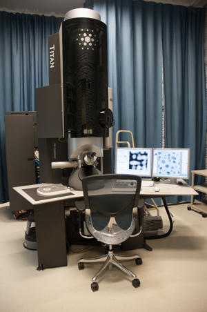
Photograph of the FEI Titan 80-300 analytical electron microscope.
The FEI Titan 80-300 scanning transmission electron microscope (STEM) is an advanced analytical field emission scanning transmission electron microscope capable of atomic-level imaging and analysis on a wide range of materials and nanostructures. The Titan is equipped with an electron energy loss spectrometer and an x-ray energy dispersive spectrometer for elemental and chemical analysis of materials at high spatial resolution. The microscope system includes a scanning module and a high angle annular dark field detector for scanning transmission electron microscopy (STEM) and for chemical analysis of very small volumes.
Specifications/Capabilities
- Acceleration voltage range: 80 kV to 300 kV with preset alignment for 80 kV, 200 kV, and 300 kV
- Scanning transmission electron microscopy mode
- Convergent beam and selected area electron diffraction modes
- Conventional TEM modes
- Point-to-point spatial resolution in TEM mode: 0.20 nm at 300 kV
- STEM resolution: 0.136 nm at 300 kV
- Super-twin objective lens pole piece
- Gatan Orius digital camera (2k x 2k)
- Gatan OneView IS CMOS camera (4k x 4k)
- Fischione high angle annular dark field STEM detector for Z-contrast imaging
- Gatan QuantumSETM energy filter for electron energy loss spectroscopy and energy-filtered TEM; filter energy spread: 0.8 eV
- EDAX Si(Li) x-ray energy-dispersive spectrometer; energy resolution: 0.136 eV
- Tomography acquisition, reconstruction, and analysis software
- Analytical, heating, cooling, and tomography specimen holders
Usage Information
Sample Restrictions:
- Thickness in region of interest: 100 nm or less
- Maximum sample size: 3-mm diameter, 100 µm thick (including TEM specimen grid)
- Materials to be analyzed must be approved by the NanoFab staff.
- No magnetic materials.
- Biomaterials must be biosafety level 0 (BSL-0). Toxic or potentially infections biomaterials are not allowed.
Typical Applications
- Atomic-level imaging and analysis of nanomaterials and nanoparticles
- Characterization of carbon nanotubes and graphene
- Characterization of semiconductor devices and interfaces
- Imaging and analysis of BSL-0 biomaterials
- Tomographic imaging