
Official websites use .gov
A .gov website belongs to an official government organization in the United States.
Secure .gov websites use HTTPS
A lock (
) or https:// means you’ve safely connected to the .gov website. Share sensitive information only on official, secure websites.
NanoFab Tool: Oxford Plasmalab 100 Inductively Coupled Plasma (ICP) Silicon Etcher
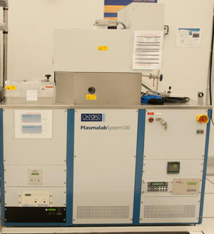
The Oxford Plasmalab 100 inductively coupled plasma (ICP) etcher is a multipurpose fluorocarbon based system that provides users anisotropic etching of silicon, silicon oxide, and other dielectric materials. The tool is equipped with a temperature controlled electrode to help users tailor their etch feature profiles. The manual load system can accommodate substrates ranging from 200 mm diameter wafers down to small pieces.
Specifications/Capabilities
- Inductively coupled plasma (ICP) power source: up to 2500 W at 2.4 MHz.
- Radio frequency (RF) power source: up to 600 W at 13.56 MHz.
- Electrode temperature range: -150 °C to 300 °C.
- Process Gases: Ar, He, N2, O2, H2, CF4, C2F6, C4F8, CHF3 and SF6
- Anisotropic etching of silicon, silicon oxide and silicon nitride.
- Low temperature silicon etching.
Usage Information
Supported Sample Sizes
- Maximum wafer diameter: 200 mm (8 in).
- Wafer diameters: 75 mm (3 in), 100 mm (4 in) - default, 150 mm (6 in), and 200 mm (8 in).
- Small pieces supported: Yes.
Typical Applications
- Silicon and silicon oxide stack etching.
- Optical device fabrication.
- General device patterning.