
Official websites use .gov
A .gov website belongs to an official government organization in the United States.
Secure .gov websites use HTTPS
A lock (
) or https:// means you’ve safely connected to the .gov website. Share sensitive information only on official, secure websites.
NanoFab Tool: ASML PAS5500/275D Stepper
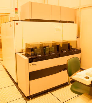
The ASML PAS 5500/275D is a high throughput i-line stepper. It utilizes 5X reduction and projection capability with step and repeat to transfer photomask patterns onto user substrates using 365 nm wavelength light and is capable of 280 nm resolution. The fully automated wafer handling system can accommodate substrates ranging from 200 mm diameter wafers down to small pieces.
Specifications/Capabilities
- Reticle size: 152.40 mm x 152.40 mm.
- Reticle thicknesses supported:
- 3.05 mm (0.12 in).
- 3.81 mm (0.15 in).
- 6.35 mm (0.25 in).
- Maximum field sizes: 22 mm x 22 mm or 27.4 mm x 14.7 mm.
- Resolution: = 280 nm.
- Overlay accuracy: = 40 nm.
- Numerical aperture: 0.48 to 0.60.
- 3D backside alignment.
- Transparent substrate processing.
- Computer programmed image distribution and die size optimization.
- Fully automated material handling and step and repeat exposure.
- Throughput: = 84 wafers per hour.
Usage Information
Supported Sample Sizes
- Wafer diameters: 75 mm (3 in), 100 mm (4 in) - default, 150 mm (6 in), and 200 mm (8 in).
- Maximum thickness: 1 mm.
- Small pieces can be processed on carrier wafers.
Typical Applications
- Measurement calibration patterns.
- Gratings and waveguides.
- Microelectromechanical systems.
- Thermal sensors.