
Official websites use .gov
A .gov website belongs to an official government organization in the United States.
Secure .gov websites use HTTPS
A lock (
) or https:// means you’ve safely connected to the .gov website. Share sensitive information only on official, secure websites.
Summary
The Waveform Metrology Project provides measurement and algorithmic support for waveform traceability to the optics and high-frequency electronics industries. NIST was the first to develop the electrooptic sampling (EOS) phase calibration of photodiodes and map this calibration into waveform measurements with uncertainty and continues to invent, develop, and provide tools for fundamental traceability and statistical analysis of high-speed signal generation and measurement while providing quality measurement services to NIST’s internal and external customers. This effort relies on 3 primary areas: optical measurement techniques, waveform processing and analysis, and development and characterization of physical device artifacts.
Description
Optical measurement techniques:
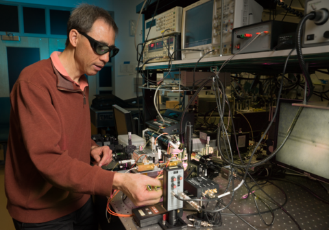
NIST uses the electro-optic sampling (EOS) technique to measure the vector response of photodiodes and provide phase traceability for commercial instrumentation, such as large-signal network analyzers, lightwave component analyzers, vector signal analyzers, oscilloscopes, pulsed laser radiometers, optical time-domain reflectometers. NMIs in South Korea, China, Germany, and the U.K. are actively working on developing similar waveform measurement services, so it is imperative to validate results from NIST and other NMIs through comparisons. Ongoing research on this traditional EOS technique includes extending the traceability beyond 100 GHz.
The electro-optic sampling system developed at NIST has revolutionized the ability to characterize the frequency response of high-speed devices from 0.25 GHz to beyond 110 GHz. However, mechanical issues coupled with synchronous sampling create a long-duration measurement that is susceptible to drift. Asynchronous optical sampling (ASOPS) techniques can be employed using two frequency combs with slightly different repetition frequencies to overcome these issues. When both combs are mixed onto a photodetector, they produce an RF comb at a different frequency. The use of dual-comb ASOPS eliminates the moving translation stage that leads to small misalignments in the conventional system and allows finer frequency resolution. The coherence of the comb allows for improvement of the signal-to-noise by employing coherent averaging or real-time phase correction methods.
It has long been the desire to image the propagation of an electrical wave along the length of an on-wafer transmission line. NIST is demonstrating a new type of EOS that measures the electric field along a CPW. Our long-term goal is to use this technique in a probe head to measure forward and reflected waveforms up to several hundreds of gigahertz.
Waveform Processing and Analysis:
The characterization of communications systems requires the measurement and characterization of waveforms that error sources that are correlated in time and frequency. These waveforms require careful analysis to properly account for and propagate uncertainties accurately. CTL researchers in this project have historically pushed the state of the art in the analysis and uncertainty quantification of noisy time-domain waveforms. Such algorithmic innovation has helped in providing waveform traceability to the optics and high-frequency electronics industries.
Under our “full waveform metrology” program, full waveforms as functions of both time and frequency are the target measurements. From these functional waveforms, traditional parametric descriptions can be derived. Furthermore, we give temporal waveforms and their frequency-domain representations consistent and equal consideration, with traceability to the International System of Units. To support this traceability, we emphasize voltage and current waveforms, their relationships, and the ability to transform both nominal values and their uncertainties from one domain to the other.
Full waveform metrology can require measurements in a variety of instruments. Some operate in the time domain, such as oscilloscopes, while others operate in the frequency domain, such as vector network analyzers. Furthermore, time-base corrections and finite bandwidth effects must be taken into account. Thus, traceability and correlated uncertainty analysis that can be propagated through each portion of the measurement process is required to maintain consistency when mapping back and forth between the time- and frequency domains.
Characterization of wireless systems requires traceable multichannel modulated-signal measurements. In principle, these measurements can be performed by large signal network analyzers (LSNAs), vector signal analyzers (VSAs), and equivalent-time sampling oscilloscopes. Traceability for each of these instruments is achieved with different traceability paths; each uses different triggering methods, and each instrument has different measurement restrictions. For example, the LSNA can be configured to make completely traceable mismatch-corrected modulated-signal measurements in a single step while oscilloscopes and VSAs must be used in conjunction with a vector network analyzer (VNA) to perform the mismatch corrections. VSAs and now even LSNAs can measure modulated signals in an epoch of longer duration than equivalent-time sampling oscilloscopes. In addition, the triggering for VSAs is more flexible than LSNAs and oscilloscopes. NIST is comparing these instruments to better understand their advantages.
Next Generation Standards:
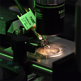
As electronic test equipment increases in frequency, higher frequency calibrations are required to validate the measurements. Commercially available photodiodes that are currently used for waveform traceability (absolute phase and relative magnitude) are limited by both the bandwidth of the device and the 1.0 mm output connector. Using a photodiode with an adapter to 0.8 mm is under validation, but the absolute magnitude response above 110 GHz is unknown and it is not an extensible approach to even higher frequencies. Through the NIST on a CHIP program, we have previously developed photodetectors up to 1 THz and strategies on how to package these devices. This opportunity allows us to develop pulse sources that are not commercially available and apply them to our metrology needs.
Calibration Services Provided:
- Fast Repetitive Pulse Parameters - for measuring the impulse response of sampling oscilloscopes (samplers) and the output of calibration-grade signal generators such as pulse generators, digital pattern generators, arbitrary waveform generators, comb generators, and vector signal generators.
- Special Test for Impulse Response Measurements of Detectors – for characterizing the vector (magnitude and phase) response of connectorized 1550 nm photodiodes up to 110 GHz using the electro-optic sampling technique.
- Frequency Response Measurements of Photodetectors – for characterizing the magnitude response of connectorized 1550 nm photodiodes up to 75 GHz using the heterodyne technique.
- Low-Level Laser Radiometer Calibration (1064 nm) – for characterizing radiometers used to measure the pulse energy and peak power of low-level 1064 nm laser pulses.
- Low-Level Laser Radiometer Calibration (1550 nm) – for characterizing radiometers used to measure the pulse energy and peak power of low-level 1550 nm laser pulses.
Major Accomplishments
- Unique electro-optic sampling system, traceable to fundamental SI units, to calibrate photodiodes up to 110 GHz.
- First calibration of complex frequency response and time-domain impulse response of an oscilloscope with mismatch corrections and full point-by-point uncertainty analysis in both the time and frequency domains that is traceable to fundamental SI units.
- Developed software to correct for both random and systematic time base errors in high-speed sampling oscilloscopes.