
Official websites use .gov
A .gov website belongs to an official government organization in the United States.
Secure .gov websites use HTTPS
A lock (
) or https:// means you’ve safely connected to the .gov website. Share sensitive information only on official, secure websites.
Summary
ZnO nanowires (NWs) are grown on bulk copper by chemical vapor deposition. Photoluminescence (PL) microscopy revealed band gap emission at 380 nm and a more intense visible emission around 520 nm due to defect states. High-resolution transmission electron microscopy shows that the ZnO NWs are single crystalline with hexagonal structure. Auger electron spectroscopy and energy dispersive X-ray spectroscopy reveal that copper is present along the length of the NW and that the surface is oxygen rich. The surface concentration of zinc increases from the tip toward the base of the NW while the concentration of oxygen decreases. Copper not only remains at the tip of the growing NW but also acts as a dopant along the length of the NW, leading to a decrease in the intensity of the band gap PL.
Description
The lasing capabilities and piezoelectric properties of single ZnO nanowires offer promise for future technologies. However, the photoluminescence of ZnO nanowires differs depending upon the synthesis method and the defects present in the sample. This project was undertaken to characterize zinc oxide nanowires mass-produced on copper supports, a nanostructure of potential interest to manufacturers of UV light sources, sensors, solar cells, field emission sources, and piezoelectric devices.
Chemical vapor deposition of ZnO on copper in a tube furnace held at 890 °C generates the nanowires. Scanning electron microscopy (SEM) was used to confirm nanostructure size and size distribution. High-resolution transmission electron microscopy (HR-TEM) and x-ray diffraction (XRD) were used to determine structure and morphology. Photoluminescence (PL) was used to measure optical properties; Auger electron spectroscopy (AES) and energy dispersive X-ray spectroscopy (EDS) allowed the optical properties to be correlated to the surface and bulk chemical properties, respectively.
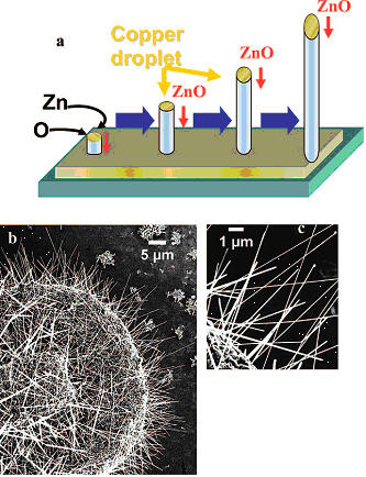
SEM micrographs of ZnO nanowires on a copper substrate are shown in Figures 1b and 1c. The growth dimensions range from 50 to 150 nm wide and from 5 to 15 μm long. The copper droplets observed at their tips confirm growth by the vapor-liquid-solid (VLS) mechanism (Figure 1a). HR-TEM confirms that the nanowires are wurtzite single crystals regardless of the growth direction relative to the substrate. The XRD spectra reveal that the lattice planes match the spacing of wurtzite. The PL spectra of the ZnO nanowires are uniform with band gap emission at 380 nm and more intense deep trap emission with a maximum around 520 nm.
EDS elemental maps show that the presence of both zinc and copper coincide with the positions of the nanowires in the SEM images, confirming copper incorporation. Enhanced copper signal at the nanowire growth termini confirm the VLS mechanism. AES spectra were collected at a series of points along the length of the nanowires. The chemical similarity between the zinc spectra from the nanowire and the starting material is notable. Comparison of the nanowire spectra to the oxidized copper suggests that the intercalated copper is chemically equivalent to the Cu2O found on the substrate. The spectral evidence also supports the formation of an oxygen-rich surface. Copper is detected along the entire length of the nanowire at ≈8% atomic concentration. From terminus to base, the atomic fraction of oxygen on the surface decreases while the atomic fraction of zinc increases. At no location does AES measure metallic Cu.
In conclusion, scanned probe electron microscopies and PL microscopy were employed to characterize ZnO nanowires produced on a bulk copper catalyst. These results indicate that the copper is expelled during growth as isolated copper ions. The entire single-crystalline structure is apparently sheathed in an oxygen-rich mixed-metal oxide whose composition is dependent upon its distance from the growth terminus. The oxygen-rich surface leads to increased deep trap emission. Copper ions that remain along the length of the nanowire are expected to lead to centers for recombination of charge carriers, leading to less intense band gap emission and more intense deep trap emission.
Major Accomplishments
- Scanning probe electron microscopies, electron-beam spectroscopies, and photluminescense microscopy were employed to fully characterize ZnO nanowires produced on a bulk copper catalyst.
- Chemical properties and optical properties of the nanowires were reconciled.
ACS Nano 2, 2, pp. 368-376 (2008)