
Official websites use .gov
A .gov website belongs to an official government organization in the United States.
Secure .gov websites use HTTPS
A lock (
) or https:// means you’ve safely connected to the .gov website. Share sensitive information only on official, secure websites.
Summary
Our goal is to develop measurements that quantify the shape, size, orientation, and fidelity of nanoscale patterns as a platform to quantitatively evaluate nanofabrication and assembly processes. NIST provides stakeholders in these fields with measurement technology that provides potential solutions to several of the Grand Challenges identified in the International Technology Roadmap for Semiconductors (ITRS) for metrology in emerging technologies that currently have no apparent solution.
Description
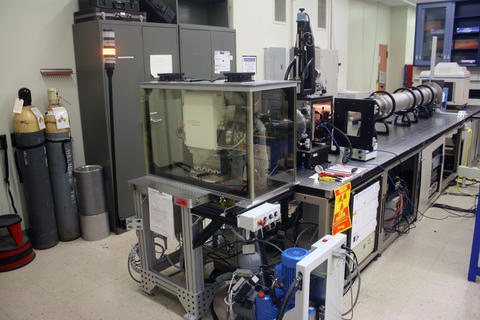

Small Angle Scattering techniques are employed to measure, with sub-nm precision, pattern shape, dimensions, and orientation for structures created in periodic arrays. Critical-Dimension Small Angle X-ray Scattering (CD-SAXS) utilizes the variable-angle transmission scattering from a small beam size (100 x 100 um) to provide detailed shape and dimensional data for 10 nm to 500 nm structures placed with high uniformity in pitch. A lab-scale prototype at NIST complements current optical scatterometry, CD-AFM, and CD-SEM methods. It can easily quantify the pattern shape in arrays of nanostructures with periodicities in the range of 10 nm to 500 nm with sub-nm precision, is non-destructive, is capable of quantifying buried or free-standing patterns, and is straight-forward to interpret via scattering theory. These unique dimensional measurements are applied to evaluate emerging nanofabrication processes including extreme ultraviolet lithography, electron beam lithography, and directed self-assembly.
Major Accomplishments
- Hosted CDSAXS short course for semiconductor industry with tutorials available online (link)
- The "Grand Challenges" of the International Technology Roadmap for Semiconductors demonstrate the lack of measurement solutions for pattern uniformity and pattern placement in dense arrays of sub-25 nm structures which are the foundation of next generation electronics and data storage.
- NIST measurements of line width roughness by CD-SAXS were quantitatively benchmarked against state-of-the-art CD-SEM in a round robin including the SEMATECH Advanced Metrology Group and Intel
- Completed CRADA with Intel on developing quantitative CD-SAXS line width and line edge roughness measurements, and measurements of 3D nanostructures
- Preliminary CD-SAXS measurements of directed self-assembly (DSA) of block copolymers for next-generation lithography to characterize the edge profile and line edge roughness. CD-SAXS measurements are being extended to resonant soft x-rays to enhance the scattering contrast between the blocks
- Lab-scale prototype instrument built for feasibility studies on NIST campus
Non-Planar Electronics:

In order to meet future challenges from thermal and power efficiency requirements of sub-22 nm technology nodes, transistor architecture is migrating from planar to non-planar structures. These structures, such as the tri-gate and FinFET products, feature increased complexity in pattern shape and nanoscale conformal coatings. Current measurement platforms are challenged by the small dimensions inherent in these structures, where diminishingly small variations in composition and dimensions will reduce or eliminate device functionality.We have used CD-SAXS to non-destructively characterize the thickness and, to a limited extent the uniformity of the thickness, of the conformal high-k dielectric layer. We have also shown CD-SAXS to be sensitive to changes in the top rounding and bottom undercut of non-planar transistor structures.
| Scattering Data | Simulated Data |
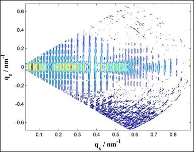 |
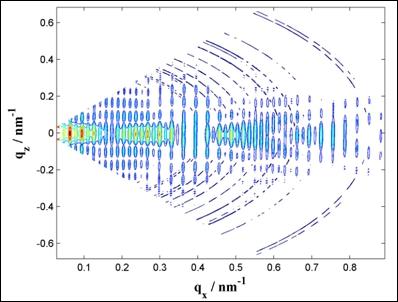 |
We have demonstrated this capability of X-ray based scatterometry by measuring high-k dielectric layers deposited from 0 to 10nm in thickness over grating patterns with a nominal critical dimension of 20 nm. For these patterns, CD-SAXS provides high precision data on average high-k dielectric thickness, line width (CD), and pitch. In addition, the measurement has the capability to measure the average top layer thickness and the dielectric thickness on the pattern sidewall independently, providing a measure of uniformity.
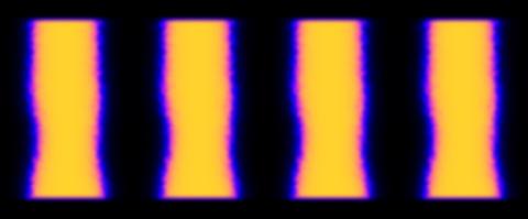
Directed Self-Assembly of Block Copolymers (DSA-BCP) for Lithography:
We have developed a suite of theory, modeling, and simulation tools in order to elucidate the morphology and thermal fluctuations in block copolymer systems for lithographic applications. Specifically, we have used polymer self-consistent field theory and stochastic polymer field theory to examine the qualitative features of lamellar block copolymer grating cross sections. These gratings—a model system for the block copolymer lithography community—were then characterized with X-ray diffraction, where the diffraction data was analyzed via a least-squared fit to a multiparameter geometric model that was constrained by our simulation results. We have also developed stochastic field theoretic methods to model and simulate the line edge roughness power spectrum in block copolymer systems, and, again, these results will be incorporated into diffraction models for line edge roughness metrology.
| Top view of DSA lamella | Edge profile of DSA lamella |
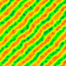 |
 |
Quantifying Scattering Data of Complex Structures through Materials Modeling Constraints:
We are currently working to seamlessly integrate materials modeling and diffraction theory into a single, cohesive diffraction analysis and fitting framework. At present, most scattering and diffraction analysis for ordered soft materials is based on complex fitting to multiparameter geometric models; for example, when fitting the diffraction pattern of a grating, the grating cross section is often modeled as a stack of trapezoids, where the number of trapezoids somehow reflects the supposed complexity of the grating cross section. The success of this approach is highly dependent on the geometric model, the initial conditions, and the fit trajectory. Furthermore, fit uniqueness is never guaranteed and seldom assumed. If, on the other hand, scattering theory were coupled to a materials model, then the grating shape would be dictated by the physical parameters in the materials model, and the uniqueness problem, if one still exists, could rest with the thermodynamics or statistical mechanics of the materials model and not with the fit procedure. This new paradigm for scattering and diffraction analysis has the potential to elevate traditional scattering and diffraction measurements in soft materials to a quantitative dimensional metrology.
Project Summary (PDF)