
Official websites use .gov
A .gov website belongs to an official government organization in the United States.
Secure .gov websites use HTTPS
A lock (
) or https:// means you’ve safely connected to the .gov website. Share sensitive information only on official, secure websites.
Summary
| This project will provide data and materials measurements necessary to improve the reliability of solder interconnects degraded by the switch to lead-free technology. In particular, the state of compressive stress and the localized creep response (whisker growth) of tin-based lead-free electrodeposits are being measured. Industry will use these measurement methods and data to modify processing conditions to prevent the formation of tin-whiskers. |
|
Description
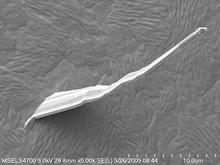
Tin is widely used as a coating in the electronics industry because it provides excellent solderability, ductility, electrical conductivity, and corrosion resistance. Unfortunately, tin whiskers often grow spontaneously from pure tin electrodeposits and short-circuit finely pitched electrical components. Adding a few percent lead inhibits whisker growth, but environmental concerns have resulted in a demand for lead-free (Pb-free) surface finishes, and an attendant demand for whisker-mitigation strategies.
|
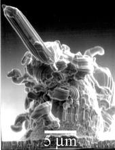
Two conditions in the tin coating are necessary, but not sufficient, requirements for whisker growth. First, a compressive stress must exist in the film. Second, energy relaxation mechanisms such as grain growth and recrystallization must be impeded, e.g., by grain-boundary pinning. We are investigating a number of strategies to prevent tin whisker formation, including the elimination of columnar grain shape through pulse deposition techniques and suppressing the intermetallic reaction of tin with the substrate. Our focused ion beam (FIB) milling has revealed this internal microstructure. We have also developed models of stress accumulation and relaxation, enabling interpretation of x-ray and cantilever beam stress measurements and a coherent description of whisker growth. |
Major Accomplishments
Work on Pb-free electrodeposits is focused on grain structure modification as a whisker mitigation strategy, and the measurement of stress using cantilever beam bending and x-ray diffraction methods. Although it is easy to obtain stress values from these techniques, understanding the source of measurement errors and the interpretation of the results is underdeveloped.
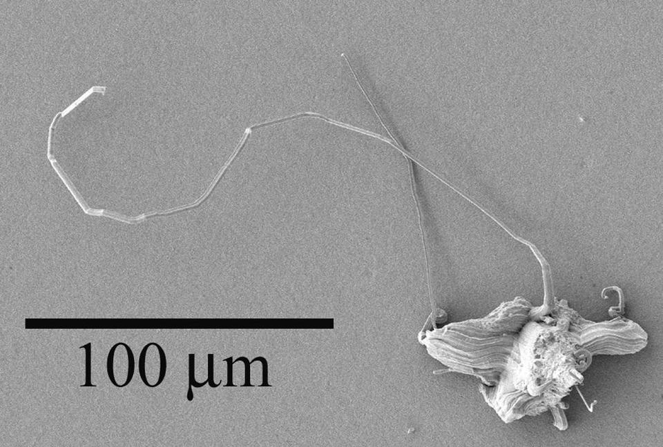
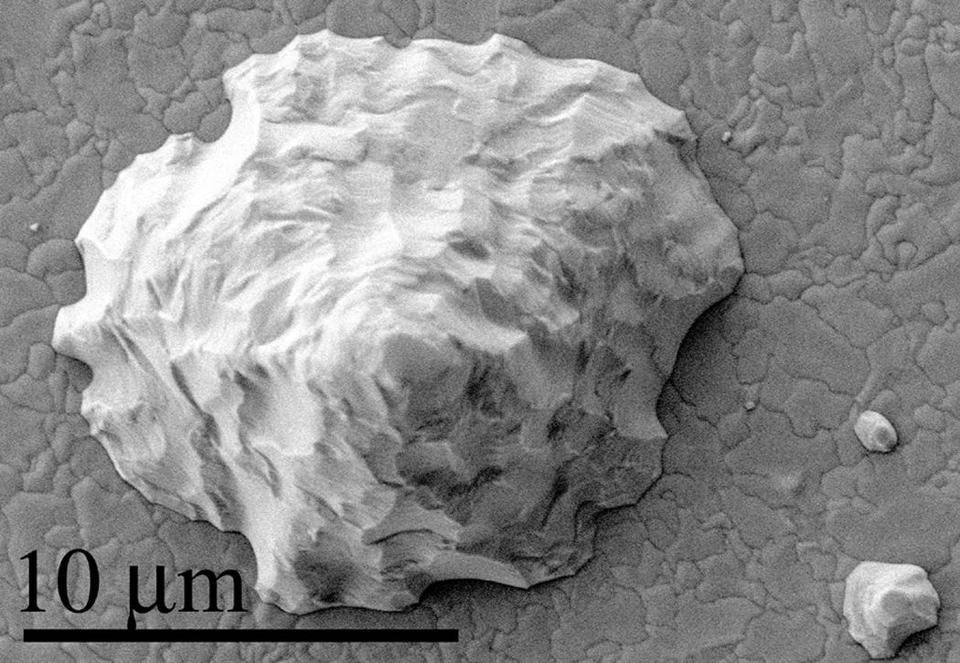
Tin whisker
Results show that the columnar grain structure of Sn electrodeposits can be modified to an equiaxed structure by pulsed deposition combined with the addition of 3 at.% Bi. Pulsed deposition is used to selectively turn on and off the Sn deposition reaction. Bi is more noble than Sn. Thus during the off cycle a displacement reaction between metallic Sn on the electrode surface and Bi+3 in solution selectively dissolves Sn and deposits Bi, effectively terminating the growth from the previous cycle and forcing the Sn to nucleate a new grain on the Bi-enriched surface. The grain size is tuned by varying the pulsing conditions, and an equiaxed structure can be obtained. This surface enrichment of Bi by potential modulation pulsed deposition is similar to that which occurs naturally in Sn-Pb deposition, and provides an avenue for breaking up the columnar grain structure inherent to pure Sn. An equiaxed grain structure enables uniform creep, rapid stress relaxation and prevents whisker and hillock formation.
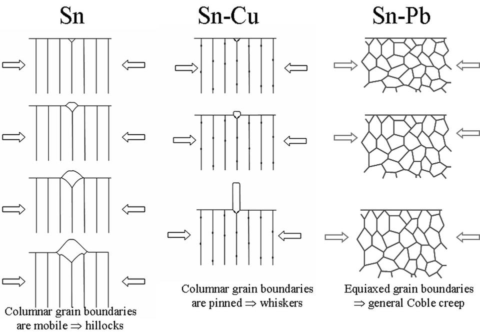
Effect of grain shape and mobility on whisker and hillock formation
Compressive stresses drive whisker formation. The origin of intrinsic electrodeposition stresses is influenced by many factors including current density, alloy formation, deposition bath additives and deposit thickness. Others have suggested that the stress arising from room-temperature formation of the Cu6Sn5 intermetallic compound (IMC) at the interface between the electroplated Sn and the Cu substrate is the sole driving force for the growth of Sn whiskers.
To test this hypothesis, one needs to separate the effects of intrinsic deposition stress from the stress generated by IMC growth. Sn and Sn-Cu alloys were plated on Tungsten (W) substrates that do not form IMC. Whiskers and hillock formed solely due to the intrinsic deposition stress but with reduced density and/or length. The claim by various authors that IMC formation is the unique cause of whisker growth is thus disproved.
Stress in the Sn was measured by electrodepositing these materials on cantilever beams made of either Cu or W. The deflection of the cantilever beam is a measure of the average stress in the film. To complement the stress measurements obtained by the cantilever beam deflection method, residual stress in electroplated Sn deposits was measured using the sin2Ψ x-ray diffraction method. The preferred orientation of the deposits and the low stress levels (~ 10 MPa) presented many challenges for this technique. A detailed analysis of errors in the measurement method as it applies to Sn has been performed. Also a major summary of whisker/hillock growth in response to intrinsic electrodeposition stress and IMC generated stress has been published.
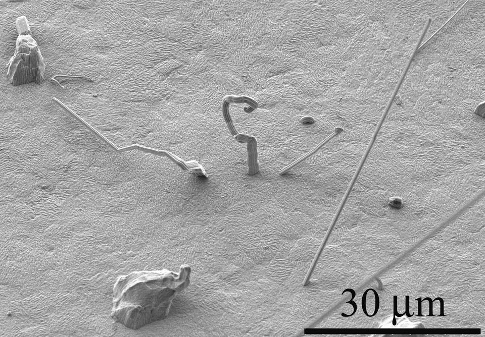
Tin hillock
Project Summary (PDF)