
Official websites use .gov
A .gov website belongs to an official government organization in the United States.
Secure .gov websites use HTTPS
A lock (
) or https:// means you’ve safely connected to the .gov website. Share sensitive information only on official, secure websites.
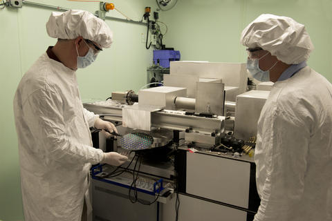
Bryan Barnes (left) and Rick Silver (right) load a wafer into the NIST-built 193 wavelength microscope.
As device manufacturing technologies sizes shrink beyond 22 nm and increase in complexity, defects become more detrimental to device performance and harder to detect. PML scientists have developed a technique to create a 3D image quickly and non-destructively that can enable fast detection of defects at the nanometer level.
Even when just a few nanometers in size, a defect can be destructive, ruining devices and negatively affecting a company's manufacturing yield. But, while detection of these tiny defects is critical, the act of finding a nanometer-sized defect on a 300 mm semiconductor wafer is daunting.
Rick Silver, leader of the Semiconductor and Dimensional Metrology Division's Surface and Nanostructure Metrology Group, explains: "The analogy is, in America you have under an hour to determine if one shoe has been misplaced. That's the challenge. One foot in 3,000 miles is identical a 10 nm defect over a 300 mm wafer."
The International Technology Roadmap for Semiconductors, a set of documents that assesses the semiconductor industry's future technology requirements, shows defect inspection in shrinking devices as being without known solutions just two years from now. Silver and his colleague Bryan Barnes, along with many others at PML, are working with major manufacturers and suppliers to evaluate and develop new techniques to meet these needs. The key to this challenge is finding a technique with high throughput that provides enough resolution to pinpoint these nano-sized defects.
"Companies need to perform measurements over large areas and they use optics to very quickly find out if a defect exists," Barnes describes. "Then, they move off the line and take the wafer to an SEM (Scanning Electron Microscope) and measure it to find out exactly what type of defect it is. We need the ability to inspect these 300 mm and 450 mm wafers quickly, cheaply, and non-destructively. The SEM is a fantastic tool for high-resolution review and root cause analysis, but it cannot review the vast area of the wafer surface quickly enough for high throughput. Optics are needed."
Silver and Barnes have taken a huge step toward solving this problem with their recent breakthrough of 3D defect detection.[1] Their technique relies heavily on the use of scatterfield optical microscopy measurements, a technique invented at NIST over five years ago. Scatterfield microscopy uses structured or engineered illumination tailored to the target of interest. The target is illuminated from various angles using selected combinations of both transverse-magnetic and transverse-electric polarizations. The combination of the structured illumination and target results in a three-dimensional interference field above the sample.[2]
The 3D detection process was completed using a NIST-developed 193 nm wavelength microscope. Silver and Barnes ultimately determined, however, that the process can be replicated on any Köhler illuminated microscope with fine control of the focus position. In other words, companies won't necessarily have to replace their expensive equipment.
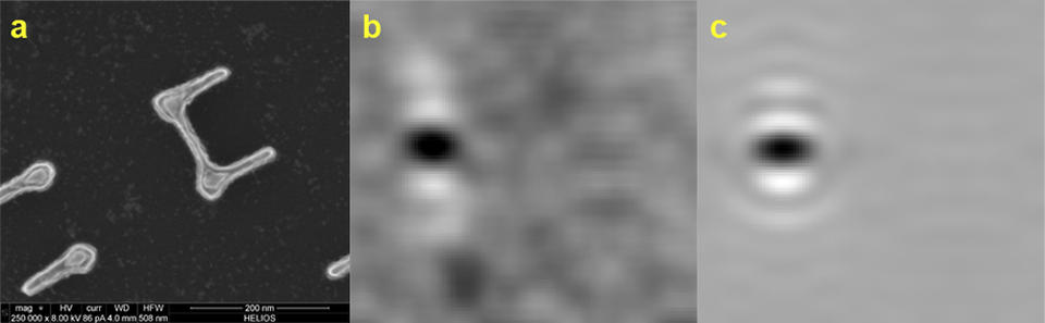
Measurements were made on an intentional defect array, created and supplied by SEMATECH, that was specifically designed to simulate upcoming challenges for the inspection of circuits with nearly 9 nm linewidths. The array included a variety of defects including bridge connection errors and line breaks. Difference volumes were generated from a comparison of the defect volume versus a reference volume.
In measuring the array, the scientists examined the interplay among the polarization, wavelength, incident angle, and focus position. Silver and Barnes collected a selection of several images through best focus. They correlated the experimental images in the x, y, and z planes and subtracted the volumes to produce a final measurement of the array.
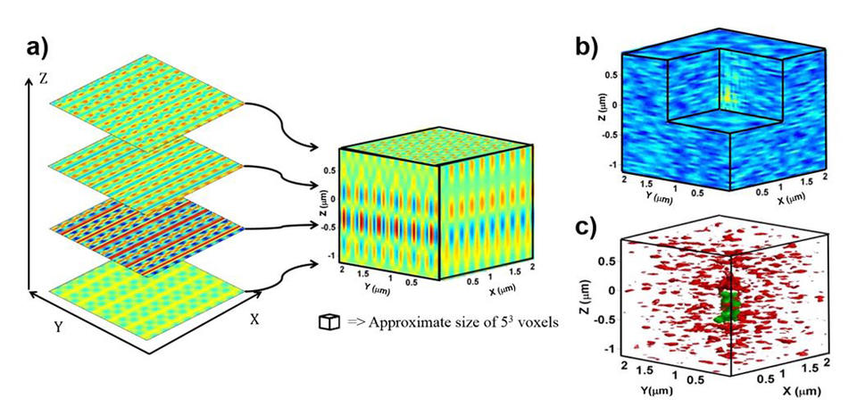
Using software that was developed in-house, they were able to combine and align these image slices using algorithms and scripts, producing a 3D volume that more accurately represented the precise locations of the defects.
The process yielded an improvement in defect sensitivity (vs. 2D imaging) that can be five-fold or greater than conventional methods. Just as importantly, the entire process shows considerable promise for identifying hard-to-detect defects otherwise not visible using a single 2-D image alone.
These successful simulations have demonstrated the ability to identify defects at a smaller scale than what is currently needed by industry. This bodes well for the future as devices shrink further and become even more complex. Still, challenges remain.
"There's no question at 10 nm that we can see defects," Silver states. "My guess is that 6 nm is also doable. The key question is the complexity of the stack. That will mask things. Every layer of complexity adds variability and background signal."
Silver and Barnes will continue to tackle these challenges, sharing their results with an industry that is eager for answers.