
Official websites use .gov
A .gov website belongs to an official government organization in the United States.
Secure .gov websites use HTTPS
A lock (
) or https:// means you’ve safely connected to the .gov website. Share sensitive information only on official, secure websites.
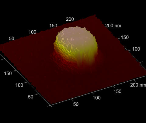
This tiny silicon pillar, measuring less than 100 nanometers along any of its sides, is the sort of computer chip feature that manufacturers now can measure more precisely with NIST's hybrid metrology method, which can reduce the nagging uncertainties that have long plagued industry's measurement efforts.
A refined method developed at the National Institute of Standards and Technology (NIST) for measuring nanometer-sized objects may help computer manufacturers more effectively size up the myriad tiny switches packed onto chips' surfaces. The method*, which makes use of multiple measuring instruments and statistical techniques, is already drawing attention from industry.
Nothing in life may be certain except death and taxes, but in the world of computer chip manufacturing, uncertainty is a particularly nagging issue, especially when measuring features smaller than a few dozen nanometers. Precision and accuracy are essential to controlling a complex and expensive manufacturing process to ensure the final chips actually work. But features on modern chips are so tiny that optical microscopes cannot make them out directly. Metrologists have to use indirect methods, like "scatterometry"—deducing their shape from sampling the pattern light creates as it scatters off the features' edges. When this isn't enough, there's atomic force microscopy (AFM). It's expensive and slow, but it can give distinct measurements of the height and width of a nanoscale object while light scattering occasionally has trouble distinguishing between them.
Even with these measurement techniques, however, there's always a nagging margin of error. "Maybe scatterometry tells you the width of an object is 40 nanometers, but it's plus or minus three nanometers, a relatively large variance," says NIST scientist Richard Silver. "Making things worse, the total uncertainty usually increases when measurement techniques are combined, making our vision even hazier."
What the NIST team needed was a more precise yet less expensive method of measuring what sits on a chip, and their answer has turned out to be a combination of scanning techniques and statistical analysis. They first created a library of simulated data based on typical chip feature dimensions to which they can compare their actual measurements, made with AFM, scatterometry and other means. A complex statistical analysis of library values is then compared with actual measurements to extract valid measurement values—but this is often at a cost of high uncertainty.
But NIST statistician Nien Fan Zhang found an elegant way to use a statistical method called Bayesian analysis to incorporate a few key additional measured values from other tools into the library model before performing the comparison. In doing so, the team was able to reduce the uncertainty in some of the measurements, lowering them by more than a factor of three in some cases. This approach is expected to be essential when measuring complex three-dimensional transistors 16 nanometers in size or smaller in the near future.
The math wizardry is a little counter-intuitive. "In essence, if you've got a really small uncertainty in your AFM measurement but a big one in your optical measurements, the final uncertainty will end up even smaller than either of them," says Silver. "IBM and GLOBALFOUNDRIES have already begun developing the technique since we first described it at a 2009 conference, and they are improving their measurements using this hybrid approach."
*N.F. Zhang, R.M. Silver, H. Zhou and B.M. Barnes. Improving optical measurement uncertainty with combined multitool metrology using a Bayesian approach. Applied Optics, Vol. 51, No. 25. Sept. 1, 2012. DOI: http://dx.doi.org/10.1364/AO.51.006196