
Official websites use .gov
A .gov website belongs to an official government organization in the United States.
Secure .gov websites use HTTPS
A lock (
) or https:// means you’ve safely connected to the .gov website. Share sensitive information only on official, secure websites.
Summary
Tunnel junctions, single electron transistors and superconducting resonators are fabricated using ultra-high vacuum metals’ deposition and in situ low energy plasma processing. These devices are then measured at cryogenic temperatures as precursors to more complex hybrid quantum devices incorporating MOS (metal-oxide-semiconducting) qubits. In particular, devices utilizing aluminum oxides (AlOx) formed in ultraclean environments with plasma oxidation exhibit reduced densities of defects promising for use in quantum devices. Aluminum oxide is a critical material in quantum devices both as a tunnel barrier material for superconducting quantum devices and as a gate oxide for surface gate in MOS devices. Below are highlights of the experimental system and the measurements of long time tunnel junction stability, Al/AlOx/Al single electron transistor devices and bilayer superconductor densities-of-state (DOS).
Description
MBE System
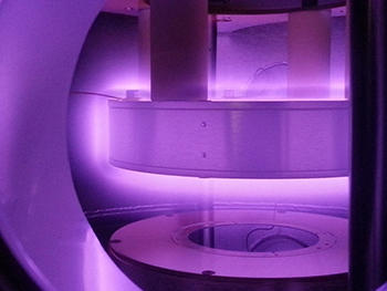
Our fabrication system is composed of ultra-high vacuum (UHV) chambers that support the in-vacuum exchange of 75 mm wafers without exposure to air as seen in Figure 1. These chambers are: (1) a deposition chamber with electron gun deposition, UHV compatible sputter guns, in situ shadow mask device definition and variable wafer temperature; (2) a UHV plasma chamber for cleaning and reacting metal films as seen in Figure 2; (3) a high-resolution UVS/XPS chamber with micro-spot capability; and (4) a load lock that can exchange up to (12) wafers or masks at a time.
Months long stability of ultrathin AlOx tunnel junctions
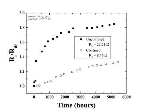
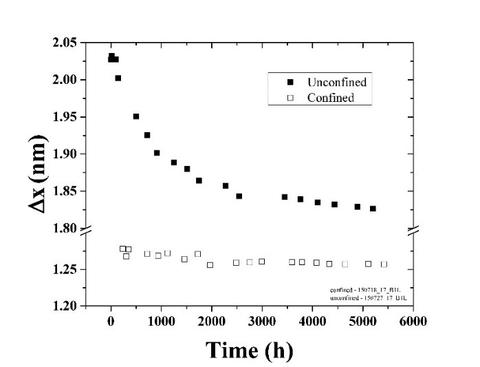
A gross property indicating device quality is the stability of the DC electrical resistance over time, in this case more than half a year. Plasma oxidized aluminum was incorporated as tunnel barriers and the longtime resistance (Figure 3) was found to be very stable, and even better when incorporating enthalpy confinement (confined devices are Co/AlOx/Co; unconfined Co/AlOx/Al). The high yield of atomic oxygen radicals in the plasma, compared to molecular oxygen in thermal oxidation processes, allows a more complete and stable stoichiometry to be achieved, resulting in less relaxation over time. Additionally, the aluminum’s more negative oxidation enthalpy compared to the cobalt results in a more stable oxygen configuration when the tunnel barrier is bounded by cobalt. This conclusion is supported by data in Figure 4, where the tunnel barrier thickness as determined by WKB fits to transport measurements (resistance vs bias) are stationary for the confined case but relax for the unconfined case. These results indicate plasma oxidation and confinement each can improve aluminum oxide quality, reducing charge defect densities.
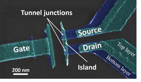
Single electron transistors (SETs) using plasma oxidized aluminum
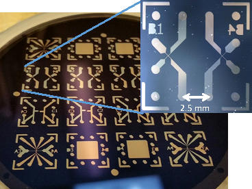
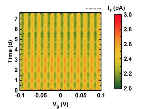
Since plasma formed AlOx was found to be very stable in tunnel junctions (above), we incorporated this material into Al/AlOx/Al single-electron-transistors (SETs), which have exquisite (sub 1 electron) sensitivity to charge instability. The SET devices were made using a resist mask defined by electron beam lithography and then loaded into our system for multiple evaporations at different angles with plasma oxidation between. A device similar to the one used for measurements is shown in Figure 5. Electrical measurements made at ~10 mK are shown in Figure 6, where the current in the gate voltage (Vg) direction exhibits Coulomb blockade oscillations. The gate voltage sweeps are made repeatedly so the oscillations form vertical stripes in the image on the right, which corresponds to an integer electron charge number on the SET island. The reproducibility of the charge configuration with gate voltage over more than a week demonstrates very good stability, nearly as good as the best silicon SET devices. The next step for these aluminum SET devices is to directly incorporate them with MOS devices and demonstrate compatibility when used as capacitively coupled charge sensors.
Al/Nb superconducting bilayers with plasma oxidized aluminum
Aluminum oxides are critical to the performance of superconducting quantum information devices, which often use Al/AlOx/Al Josephson junctions. Niobium is another desirable elemental superconductor but has very poor oxides. In this study, we are depositing aluminum on niobium superconducting bilayers and using plasma oxidation in order to achieve the high Tc (superconducting transition temperature) of niobium while retaining the high-quality tunnel junctions from plasma oxidized aluminum. A question that emerges is “how do the superconducting states of the bilayer evolve, as the thickness of the aluminum is changed, when measuring in a temperature regime between the bulk Tc of Al and the bulk Tc of Nb?”
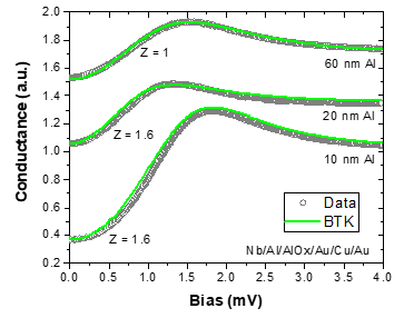
To study this question, we have grown normal-insulating-superconducting junctions (NIS) using Al/Nb bilayers with plasma oxidized aluminum and measure the state properties using tunneling density of state (TDOS) measurements (Figure 7). The thickness of the aluminum is varied while the Nb is kept at 40 nm, revealing the evolution of the superconducting state as the upper layer thickness is changed, e.g., the zero bias conduction is seen to increase, possibly due to a change in the reflection probability of the states.
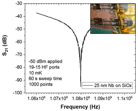
Additionally, we are currently developing devices and measurements to demonstrate technologically relevant performance in the microwave regime. We expect to implement these same high-quality materials into technologically relevant devices. As a first example, an LC (inductor-capacitor) resonator etched from a Nb thin film with a Q > 6000 is mounted and measured on a microwave coplanar waveguide (see Figure 8). These structures are planned for implementation on MOS devices and incorporation of high-quality oxides to allow high bandwidth readout of charge and spin states.
Looking ahead, we plan to assemble these pieces in to hybrid combinations of MOS, superconducting and metal SET devices to realize higher technological functionality and reveal where design and material limitations inhibit improvement.
Related Blog
Seeking the Power of Quantum Computing in Silicon