
Official websites use .gov
A .gov website belongs to an official government organization in the United States.
Secure .gov websites use HTTPS
A lock (
) or https:// means you’ve safely connected to the .gov website. Share sensitive information only on official, secure websites.
Summary
We are working to fabricate and perform low-temperature measurements of CMOS-compatible single electron devices in silicon which could be used as a standard of electrical current. Our goal is to produce a current of about 10 nA from about 100 single electron devices operating in parallel with a relative error rate below 10-8.
Description
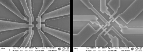
Single electron devices with integrated charge sensors in two different architectures. Left: Polycrystalline silicon gates on a bulk wafer. Right: Mesa-etched silicon-on-insulator (SOI) wafer with polycrystalline silicon gates.
Our devices can manipulate and trap a single electron in a quantum dot through the application of voltages to electrostatically controlled tunnel barriers. By cycling these voltages appropriately, we are able to sequentially pump one electron at a time through the device. To produce a current standard we run the cycle at a frequency, f, to produce a current, I=ef. This forms the basis for an electrical current standard based on the charge of the electron, a fundamental constant, and the frequency at which we run the device. When 2 or more devices are operated in parallel the current is multiplied by the number of devices. By parallelizing about 100 devices and operating at about 1 GHz we could produce a current of about 10 nA.
Efforts include:
- Understanding the source of different error mechanisms for pumping electrons. For instance, during a cycle we could erroneously pump zero or two electrons rather than one causing the current to deviate from I=ef.
- Fabricating and measuring devices with minimal defect densities to eliminate any drift in a device's operating point as well as minimizing differences in each device's response to gate voltages.
- Evaluating the effectiveness of different device architectures and designs as they relate to error rates.
*This work is done in close collaboration with the team of Neil Zimmerman and the devices produced for the current standard experiments are very similar to those used for quantum coherent experiments.