
Official websites use .gov
A .gov website belongs to an official government organization in the United States.
Secure .gov websites use HTTPS
A lock (
) or https:// means you’ve safely connected to the .gov website. Share sensitive information only on official, secure websites.
Summary
This program aims to develop standards, methods, and modeling for assessing the periodic structures using optical reflectance and transmittance measurements.
Description
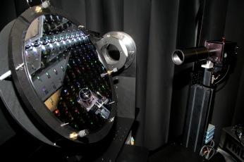
In the past few years, scatterometry has emerged as a method for performing linewidth and line profile metrology, especially by the semiconductor industry. The method uses a periodic target containing repetitive lines whose profile, i.e., its width, height, and shape, is to be determined. The technique relies on the complicated behavior that the grating structure has on the diffracted light as a function of incident angle and wavelength, and the sensitivity to small changes in the grating profile. By comparing measurements with a library of calculated model results, the profile can be inferred. While the method claims extreme sub-nanometer-level sensitivity to the line profile, there are a number of outstanding issues that the user community has regarding the technique's absolute accuracy. Some of these issues are outlined below:
- The method relies upon rigorous coupled wave analysis (RCWA) of the diffracted light. RCWA provides an accurate solution to Maxwell's equations for periodic structures, but does not address the issues of finite structures, finitely illuminated structures, or non-periodic structures. Questions thus arise about the accuracy of the method for realistic structures.
- The method relies on having accurate values for the optical properties of the materials in the structure. Issues, such as the presence of thin oxide films or near-surface optical properties, are usually overlooked.
- Standards are needed in order to validate the method. These structures would be characterized by a variety of metrologies and would provide well-characterized profiles.
- The limits of scatterometry, in terms of how long it will remain a viable solution to the semiconductor industry's needs as device dimensions are reduced, are unknown. It is essential that these limits be determined so that the industry can develop alternative solutions. Any advances that would extend those limits would be welcomed.
- Extensions to the scatterometry technique need to be explored. For example, the method is primarily used to assess two-dimensional profiles. Extending scatterometry to three-dimensional profiles may reduce the need for non-functioning targets, or allow measurement of line-edge and line-width roughness.
This program aims to address these and other issues both theoretically and experimentally.