
Official websites use .gov
A .gov website belongs to an official government organization in the United States.
Secure .gov websites use HTTPS
A lock (
) or https:// means you’ve safely connected to the .gov website. Share sensitive information only on official, secure websites.
Summary
We synthesize semiconductor nanostructures to serve both as test structures for measurement techniques and as building blocks for novel metrology tools and devices, with a focus on GaN nanowires. We also adapt traditional methods of semiconductor characterization for use on nanostructures to evaluate accuracy and determine best practices for those methods, including Raman spectroscopy, photoluminescence, triple-axis x-ray diffraction, and electrical device fabrication and testing.
Description
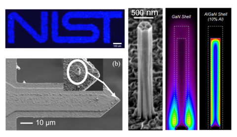
Clockwise from upper left: NIST logo illustrated with about 12,000 nanowire LEDs operated in parallel; Electron microscope image of nanowire LED and modeled light emission intensity for two different device designs; GaN nanowire on a scanning probe tip with metal contact for microwave signal detection.
GaN Nanowire LEDs: Our selective epitaxy methods and dopant characterization techniques have enabled fabrication of arrays of nanowire LEDs with controlled location and spatial layout. This development is complemented by modeling of the carrier flow and recombination. These LEDs were combined to create an on-chip optical interconnect.
Scanning probe metrology using GaN nanowire tips: A major goal of our project is to develop new metrology tools for examining the optoelectronic properties of semiconductor nanostructures. We are currently developing GaN nanowires as multifunctional scanning probe tips, combining light emission, microwave reflection, and topology measurement. The nanowires have been shown to retain their shape indefinitely, thus they are more durable than standard glass near-field scanning optical microscopy (NSOM) tips and more reproducible than state-of-the-art Pt tips for near-field scanning microwave microscopy (NSMM).
Read more about the Integrated Near-field Optoelectronic (INFO) Scanning Probe >>
Read more about GaN nanowires >>
Optical measurements of semiconductor nanowires: Using time-resolved photoluminescence (PL) and geometrical variations in nanowires, we demonstrated how to extract a surface recombination velocity. The temperature dependence of the PL lifetime in turn provided a means to measure internal quantum efficiency of GaN nanowires without resorting to inaccurate assumptions about quantum efficiency at low temperature.
Doping measurements: We have pursued multiple methods of extracting carrier concentration for GaN nanostructures, the most direct methods being free carrier concentration estimates in n-type GaN using Raman spectroscopy and terahertz absorption. Corroborating experiments including electrical resistance measurements coupled with photoconductivity and surface band bending modulation. Conductance changes were also mapped out with high-frequency scanning probes and testbeds.
High Q Nanoscale Mechanical Resonators: GaN nanowires have unusually low mechanical resonance losses for a nanoscale object. In collaboration with Prof. Charles Rogers at the University of Colorado, we have demonstrated a number of their unique properties and potential applications, such as mass sensing and temperature sensing.
FETs and Sensors: We have fabricated and tested nanowire MESFETs and MOSFETs with low subthreshold swing, and more recently demonstrated with collaborators that these devices have a high switching efficiency. The nanowires have also proven adept as functionalized chemical sensing devices and probes of liquid crystals.
GaN nanostructure arrays with calibrated reference dimensions are available as Standard Reference Instrument 6012.
Major Accomplishments
- Fabricated NSMM tips from GaN nanowires that outperform state-of-the-art Pt tips
- Demonstrated best GaN nanowire MESFET devices and single-nanowire LEDs to date
- Developed use of multiple methods to estimate carrier concentration and mobility in nanowires
- Developed reliable method for estimating internal quantum efficiency for single nanowires
- Demonstrated programmable spectral solar simulator on a variety of photovoltaic materials
- Defect-free GaN nanowires received R&D Micro Nano 25 Award for NIST in 2006