
Official websites use .gov
A .gov website belongs to an official government organization in the United States.
Secure .gov websites use HTTPS
A lock (
) or https:// means you’ve safely connected to the .gov website. Share sensitive information only on official, secure websites.
Molecular Beam Epitaxy (MBE) Facility
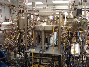
The Applied Physics Division utilizes a fully automated, dual-chamber molecular beam epitaxy (MBE) system for the growth of advanced, compound semiconductor heterostructures, composed of compounds based on GaAs, InP, and GaN, with sub-nanometer control of the film thicknesses. The MBE system is used to make nanostructures, including quantum dots and nanowires, and epitaxially layered structures, for the fabrication of lasers, photodetectors (including single photon detectors), light-emitting diodes (LEDs), and other devices for optoelectronic metrology. It is also used to grow test structures for optical, electrical, structural and mechanical measurements. The applications of the devices and structures produced by the MBE system include quantum cryptography and computing, quantum optical metrology, optical communications, nanoscale electromagnetic measurements of future-generation solar cells and LEDs, and sensors.