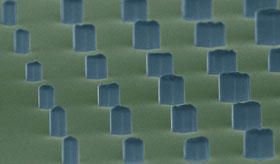
Researchers at the National Institute of Standards and Technology (NIST) have cultivated many thousands of nanocrystals in what looks like a pinscreen or "pin art" on silicon, a step toward reliable mass production of semiconductor nanowires for millionths-of-a-meter-scale devices such as sensors and lasers.
NIST researchers grow nanowires made of semiconductors—gallium nitride alloys—by depositing atoms layer-by-layer on a silicon crystal under high vacuum. NIST has the unusual capability to produce these nanowires without using metal catalysts, thereby enhancing luminescence and reducing defects. NIST nanowires also have excellent mechanical quality factors.
The latest experiments, described in Advanced Functional Materials, maintained the purity and defect-free crystal structure of NIST nanowires while controlling diameter and placement better than has been reported by other groups for catalyst-based nanowires. Precise control of diameter and placement is essential before nanowires can be widely used.
The key trick in the NIST technique is to grow the wires through precisely defined holes in a stencil-like mask covering the silicon wafer. The NIST nanowires were grown through openings in patterned silicon nitride masks. About 30,000 nanowires were grown per 76-millimeter-wide wafer. The technique controlled nanowire location almost perfectly. Wires grew uniformly through most openings and were absent on most of the mask surface.
Mask openings ranged from 300 to 1000 nanometers (nm) wide, in increments of 100 nm. In each opening of 300 nm or 400 nm, a single nanowire grew, with a well-formed hexagonal shape and a symmetrical tip with six facets. Larger openings produced more variable results. Openings of 400 nm to 900 nm yielded single-crystal nanowires with multifaceted tops. Structures grown in 1,000-nm openings appeared to be multiple wires stuck together. All nanowires grew to about 1,000 nm tall over three days.
NIST researchers analyzed micrographs to verify the uniformity of nanowire shape and size statistically. The analysis revealed nearly uniform areas of wires of the same diameter as well as nearly perfect hexagonal shapes.
Growing nanowires on silicon is one approach NIST researchers are exploring for making "nanowires on a chip" devices. Although the growth temperatures are too high—over 800 degrees Celsius—for silicon circuitry to tolerate, there may be ways to grow the nanowires first and then protect them during circuitry fabrication, lead author Kris Bertness says. The research was partially supported by the Defense Advanced Research Projects Agency (DARPA) Center on Nanoscale Science and Technology for Integrated Micro/Nano-Electromechanical Transducers (iMINT) at the University of Colorado at Boulder.
K. A. Bertness, A. W. Sanders, D. M. Rourke, T. E. Harvey, A. Roshko, J.B. Schlager and N. A. Sanford. Controlled nucleation of GaN nanowires grown with molecular beam epitaxy. Advanced Functional Materials. Published online: July 13, 2010. DOI: 10.1002/adfm.201000381

