An official website of the United States government
Here’s how you know
Official websites use .gov
A .gov website belongs to an official government organization in the United States.
Secure .gov websites use HTTPS
A lock (
) or https:// means you’ve safely connected to the .gov website. Share sensitive information only on official, secure websites.
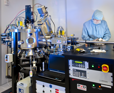
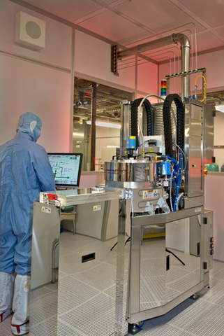
Clean room manager John Nibarger examines a wafer carrier on a new load-locked deposition tool for sputtering noble-metal materials.
After months of construction, installation, troubleshooting, and testing, the new clean room at NIST's Precision Measurement Laboratory complex on the Boulder campus is now operational.
"The expanded ability to go rapidly from invention to realization of microfabricated devices will enable the NIST-Boulder research staff to realize a wide range of breakthroughs in microfabricated quantum standards and measurement systems," says Bob Hickernell, who heads PML's Quantum Electronics and Photonics Division.
There has been a clean room at NIST/Boulder since 1971. It was rebuilt in the 1980s and continuously improved through the 1990s. But during the past decade, the burgeoning variety and volume of research had strained the 5000 square foot facility to its limits. "The equipment was shoehorned in," says John Nibarger, who manages the new clean room. "People worked shoulder-to-shoulder, and it was very difficult to access sections of the instruments. Now our users have an environment in which they can work more safely and more effectively."
"Basically, what has been done is to take a 25-year-old facility that was never built to be a true clean room, and bring it into the 21st century," says Dave Rudman, leader of PML's Quantum Devices Group. "It is clear evidence of how important microfabrication and related efforts are to NIST/Boulder that we have devoted fully one quarter of the space in our new Precision Measurement Laboratory building to this clean-room resource."
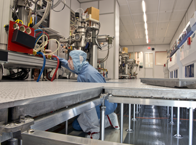
The new facility's raised floor system permits easy access to tools and wiring, and provides optimal air flow to maintain Class 100 cleanliness.
The new facility, at 18,000 ft2, more than triples the floor space of its predecessor, and has more than four times the area designated as "Class 100," referring to maximum number of particles 0.5 micrometers or larger per cubic foot of space. The numerous access corridors, or chases, between instrument arrays provide ample instrument access and contain other equipment such as the state-of-the-art toxic gas monitoring system which can detect 10 different hazardous gases used on eight different tools.
Overall, the space houses about 60 precision tools – 27 relocated from the prior facility or moved in from other labs – which will impact several key areas of metrology research and device fabrication:
Optical lithography. A new commercial-grade stepper will allow feature sizes of 0.35 μm; the previous minimum was 0.5 μm. In addition, a new pattern generator will improve the lab's ability to make its own masks.
Deposition and etching. There are 15 deposition tools – including five electron-beam evaporators, eight multilayer sputtering tools, and two kinds of tools for plasma-enhanced chemical vapor deposition of silicon dioxide and silicon nitride – and 13 dry etch tools.
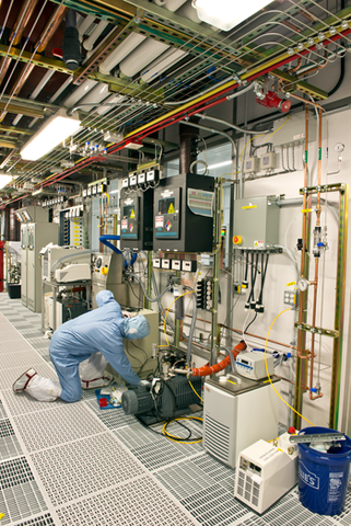
A chase between instrument bays contains utilities, pumps, and toxic gas monitoring sensors to leave the instrument bays clean and clutter-free.
MEMS fabrication. The new clean room features two four-tube furnaces, half of them atmospheric (for silicon dioxide and doping) and half are optimized for low-pressure chemical vapor deposition of silicon nitride, polysilicon materials, and low-temperature oxides. These devices provide the materials from which microelectromechanical devices are fabricated.
E-beam lithography. An existing scanning electron microscope has the capability to do rudimentary electron-beam lithography, which can produce extremely small feature sizes.
In addition, a separate section of the facility contains a new two-chamber unit for molecular beam epitaxy (MBE) with completely separate gallium nitride (GaN) and gallium arsenide (GaAs) deposition chambers.
"That will be a major benefit," says Kris Bertness of the Optoelectronic Manufacturing Group, whose team is experimenting with using nanowires as extremely tiny light sources. "We've had trouble since the beginning of the program in 2004 with our indium gallium nitride quantum well growth, and recently we were able to have atom probe analysis done. In the old system, we shared a growth chamber with the GaAs experiment, and the analysis revealed that there was arsenic in our structures. That seems to have been at least part of the problem.
"Even though we have made better single-nanowire GaN LEDs than anyone else has made with MBE, their performance is still disappointing given that most of the nanowires are defect-free and have high internal quantum efficiency. But with the new system, we should be able to make much more efficient light emitters almost right away because we will have much better control over p-type doping, among other things.
"We want to try to get to the point where we're comparable to commercial LEDs. So having a state-of-the-art machine will make a big difference."
Tools are well-spaced, allowing easy access for maintenance and use.
The new clean room's dramatically expanded resources are expected to keep NIST at the frontier of research in numerous areas where PML has unique and globally recognized expertise.
For example, NIST defines the standard volt using arrays of up to 300,000 superconducting Josephson junctions. These quantum standards are fabricated in the clean room and integrated into systems disseminated to other national metrology institutes around the world.
Another class of devices utilizing the unique properties of superconductors are transition-edge sensors (TESs) in which the energy deposited by incoming photons or particles forces the transition from the superconducting to the normal state, providing a very sensitive measure of energy. "NIST can make TESs that span over 11 orders of magnitude in energy," Nibarger says, "ranging from microwaves to gamma rays to alpha particles from nuclear decay.
"On the long-wavelength side, Kent Irwin of the Quantum Devices Group and his team have devised a sensor of unprecedented resolution that is now in use on the South Pole Telescope to study the Cosmic Microwave Background. You could characterize it as a 'deliverable' to the astronomical community. They couldn't have done that without clean-room capabilities that permit a little research and development in the course of solving problems, letting us actually fabricate and test solutions." A variation on TES design is also employed at the Atacama Cosmology Telescope in Chile.
A new silicon nitride/silicon oxide etch tool offers a capability that allows researchers to etch material in 4 minutes, versus an hour on the previous tool.Other wavelengths are suited to other TES solutions. Exquisitely sensitive single-photon detectors made possible by clean-room tools are part of an effort to provide unparalleled security for optical communications and to enable quantum optical metrology to reach resolution below the Heisenberg uncertainty limits. A new, NIST-designed x-ray detector has been installed at the National Synchrotron Light Source at Brookhaven National Laboratory; and a 256-pixel gamma-ray detector is presently in use. "That plays a major role in nuclear non-proliferation questions," Nibarger says. "There's nothing else available with that kind of fine resolution," allowing users to more clearly distinguish between isotopes and their ratios in a radiation source.
Other recent results of clean-room research and fabrication include gallium-nitride nanowires that can be placed on a probe tip to do near-field scanning optical microscopy, MRI contrast agents with color range that can return different kinds of information at different frequencies, a number of structures for potential spintronic applications, and the "atomic clock on a chip," which has just been commercialized.
Even the work of David Wineland, winner of the 2012 Nobel Prize in Physics for his studies of trapped ions, benefitted directly from NIST's clean-room tools. "Over the years, Dave kept making his traps smaller and smaller," Nibarger says, "and eventually he went down to the clean room staff to see if the traps could be configured on that scale. That began a decade of research and development that affected Dave's award-winning research."
It is impossible to predict specific accomplishments that the new facility will make possible, but PML scientists anticipate that within five years the expanded capabilities will speed progress toward numerous goals, including:
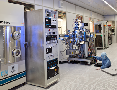
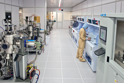
Multiple copies of similar tools, along with commodious work space, improve the facility's throughput.
Advanced multi-zone surface-electrode ion traps for quantum information processing and quantum simulation.
A new generation of high-performance microfabricated "chip scale" atomic magnetometers for use in systems to monitor magnetic fields from the human brain.
The world's most sensitive force sensors using quantum-limited micromechanical detectors.
Integrated microfluidic and microelectronic circuits for high-frequency electronic biosensors such as DNA counting devices.
Revolutionizing x-ray spectroscopy using microfabricated superconducting detector arrays to advance analysis for criminal forensic, semiconductor manufacturing and photovoltaic development.
Hybrid superconductor-magnetic cryogenic memory as the enabling technology for very low power petaflop supercomputers.
Magnetic nanoagents to allow single nanoparticles to be imaged in the human body using MRI for cancer and other disease screening and diagnosis.
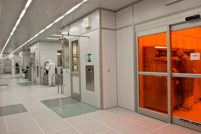
The wide central corridor permits unimpeded transit of personnel and equipment.
A new generation of cameras based on quantum-limited superconducting detector pixels for imaging the cosmic microwave background at multiple colors simultaneously, to probe for gravity waves from the Big Bang.
Gas permeation membrane standard reference materials for application in the implantable medical device industry to improve device safety.
A new class of multimeasurand near-field scanning probes to study optically generated carrier dynamics with unprecedented spatial and temporal resolution with applications ranging from beyond-CMOS electronic devices to nanoscale energy generation and storage.