
Official websites use .gov
A .gov website belongs to an official government organization in the United States.
Secure .gov websites use HTTPS
A lock (
) or https:// means you’ve safely connected to the .gov website. Share sensitive information only on official, secure websites.
Summary
Researchers in the Flux Quantum Electronics (FQE) Project exploit the inherent quantum behavior of superconductivity to develop cryogenic superconductive circuits for applications in quantum computing, wireless communications, and high-speed, energy-efficient computing. The FQE team has built the infrastructure to design, simulate, fabricate (using the NIST cleanroom), and test these high-speed digital and mixed-signal superconductive circuits all with a short cycle time, enabling rapid progress. These cryogenic circuits operate at 4 K (-269 °C) or below and are designed to generate quantized voltage pulses and manipulate quantized fluxons to precisely control quantum bits, synthesize arbitrary electrical waveforms, or perform digital computations, all with quantum-based accuracy, reproducibility, and stability. These fluxons are analogous to the "ones and zeros" on which modern digital electronics are based but are quantized and immutable, and therefore can be used to develop standards.
The FQE team is working on four main projects:
- Quantum-based reference sources and programmable waveform synthesizers in the microwave- and millimeter-wave frequency bands to provide standards for secure, tamper-proof, current and future communication technologies (e.g., 5G and 6G wireless).
- Single-flux-quantum (SFQ) microwave and mixed-signal circuits for the control and readout of quantum bits in a cryogenic quantum computer.
- Superconductor quantum circuits and SFQ “classical” circuits in support of microwave calibrations for quantum computing.
- Test and evaluation of electronic design automation (EDA) software tools for automating the complete concept-to-chip design flow for superconductor application specific integrated circuits (ASICs).
Description
Quantum-Based Reference Sources
The demand for wireless communications has exploded over the last 2 decades and there is no end in sight. The quest for higher bandwidth is driving the use of higher carrier frequencies in the microwave and millimeter-wave (>30 GHz) bands. However, there are no primary reference signal standards at these frequencies. What is used now is a receiver that measures the power of an incoming signal (e.g. a thermal voltage converter). A reference source at 5G wireless frequencies would be a game-changer, enabling faster deployment of new wired and wireless technologies.
To fulfill this need, the FQE team is developing quantum-based reference sources, programmable waveform synthesizers, and even comb generators for these frequencies. We are building on the success of NIST’s programmable Josephson Arbitrary Waveform Synthesizer(JAWS), the NIST Standard Reference Instrument for ac voltage (up to audio frequencies), and are exploring new ways to develop superconductor-based, higher-speed, accurate AWS sources for use as calibration standards. Recently, the FQE team together with the Quantum Voltage team has demonstrated several high-speed modifications to the JAWS design capable of reaching frequencies above 5 GHz. Together with the Communications Technology Laboratory, the team is developing the theory and techniques to transfer the on-wafer quantum-based accuracy to room temperature and has published calibrated measurements of the output power of these circuits for synthesized signals up to 1 GHz.
This demonstration at 1 GHz is an improvement of 100,000 times in frequency over the existing audio frequency JAWS. However, it is not fast enough to serve as a calibration tool for the full range of 5G signal frequencies. To make reference sources for these higher frequencies, FQE researchers are employing “single flux quantum” (SFQ) technology. Extremely tiny, brief, and accurate electrical output pulses are emitted from Josephson junctions when they are excited by an electrical signal. Like many properties at extremely small scales, these tiny electrical pulses are quantized – that is, they can only take on exact, discrete values, the smallest possible amount of which is a single flux quantum. And because they are quantized, their values are precisely known and equal to the ratio of two fundamental constants of nature, the key to making a reference standard.
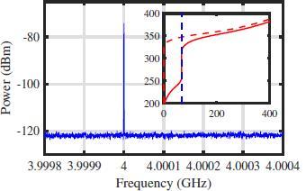
In 2018, a conceptual design for an SFQ-based “Synthesizer-on-a-Chip” (SOC) was proposed by the FQE team. In a 2021 publication, first authored by Manuel Castellanos-Beltran, key sub-circuits of that SOC have been demonstrated. Fig. 1 shows a power spectrum of a 4 GHz signal synthesized by the 8-fold voltage multiplier circuit shown in Fig. 2.
This work also supports Congress’ directive to NIST for advancing microelectronics technology and specifically for developing measurements and tools for ensuring secure, tamper-proof wireless communication systems. The FQE team is collaborating with researchers in NIST’s Communications Technology Laboratory, who are investigating “over-the-air” identification techniques, i.e. analyzing transmitted electromagnetic signals from wireless equipment and systems, to identify potential threats for secure communications. This work would benefit from a reference source that can provide a “clean” (free of noise and distortion) signal for calibrating their test equipment.
Single-Flux-Quantum Circuits for Cryogenic Quantum Computing
Quantum computing, and in particular cryogenic superconducting quantum computing with its demonstration of “Quantum Supremacy”, has made tremendous progress over the past decade with many US companies playing primary roles in this revolutionary development. However, building quantum computers powerful enough to solve useful problems will require thousands if not millions of physical quantum bits (qubits), and this scaling problem presents some substantial technological hurdles. One such hurdle is a scalable and low-latency solution for qubit control and readout electronics, avoiding the “rat’s nest” of wires and cables connecting the racks of room temperature electronics to the qubits in the cryostat.
In-situ, cryogenic single-flux-quantum (SFQ) digital electronics have been proposed and initial demonstrations have shown them to be a potential solution to this hurdle. The NIST FQE research team is investigating single-flux-quantum (SFQ) microwave and mixed-signal circuits for the control and readout of cryogenic quantum bits (qubits) in a quantum computer. This work is in collaboration with multiple NIST groups and is funded by NIST in support of the National Quantum Initiative Act and the White House National Strategic Overview for Quantum Information Science. We are also collaborating with universities and the Department of Energy in distinct but related work.
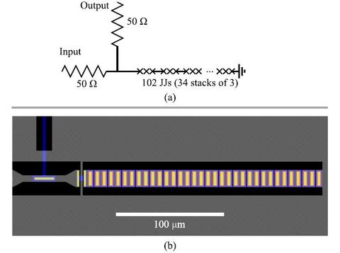
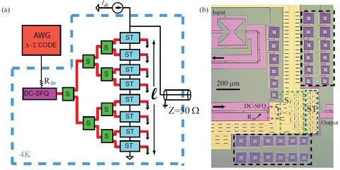
In a recent publication first-authored by Adam Sirois, the FQE team demonstrated the use of a Josephson Arbitrary Waveform Synthesizer (JAWS) circuit (Fig. 3) in a new application - for controlling a superconducting qubit. In this proof-of-concept demonstration, the team performed spectroscopy on the qubit showing the quantized energy levels of the qubit using the JAWS source located at the 4 K temperature stage and the qubit at the base temperature (< 100 mK) stage of an adiabatic demagnetization refrigerator (see Fig. 4). They also demonstrated the stable, self-calibrated, and reproducible output signal of the JAWS, a feature that allows these synthesizers to be replicated and scaled in the cryostat, all with identical on-chip, quantized, outputs.
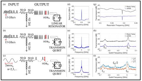
The team is currently measuring qubits and JAWS circuits in a dilution refrigerator in order to further explore the use of JAWS and SFQ-based synthesizers for the state initialization and control of coupled superconducting qubits and cavities with resonant frequencies in the 4-12 GHz range and cooled to < 30 mK temperatures. The team of Manuel Castellanos-Beltran, Adam Sirois, and NRC postdoc Logan Howe also intends to pursue scalable readout solutions using SFQ-based electronics.
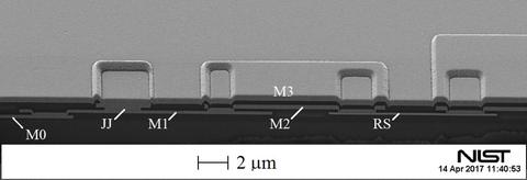
The work shown above is made possible by David Olaya and John Biesecker, who lead the fabrication process development portion of the FQE team. Using NIST’s Boulder Microfabrication Facility and working with the Quantum Voltage team, they have developed processes for fabricating JAWS synthesizers and SFQ-based circuits with large numbers of Josephson junctions (JJs) that operate at faster speeds and with higher yields. Their work allows the team to go from design to finished chips in less than a few weeks, enabling fast prototyping. Fig. 6 shows a cross-sectional image, generated by NIST’s scanning electron microscope with focused ion-beam (FIB-SEM) capability, of the layer stackup from a wafer fabricated using the NIST SFQ process on a 3” silicon substrate. It features four niobium (Nb) metal layers (M0-M3), a bias resistor layer (RS), and self-shunted JJs. The first two metal layers are fully planarized using chemical-mechanical polishing (CMP). Traditional SFQ fabrication would include an additional junction-shunting resistor, but by using our unique process for making the junctions we can create self-shunted junctions and omit that resistor, The team is currently measuring qubits and JAWS circuits in a dilution refrigerator in order to further explore the use of JAWS and SFQ-based synthesizers for the state initialization and control of coupled superconducting qubits and cavities with resonant frequencies in the 4-12 GHz range and cooled to < 30 mK temperatures. The FQE team is also pursuing scalable readout solutions using SFQ-based electronics.
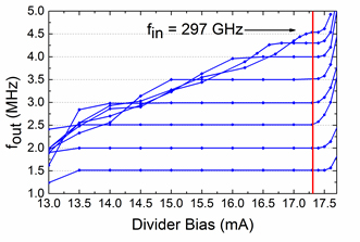
Our JJ technology is leveraged from the decades of success of the Quantum Voltage project. The voltage standard is fabricated using the same self-shunted, stacked junction process that enables more than a quarter of a million junctions to fit on a single chip and therefore produce up to 10 volts output with excellent yield. The voltage-standard chips are composed of long series arrays of stacked Nb/NbxSi1-x/Nb JJs embedded in a superconducting coplanar waveguide. This niobium-doped silicon (NbxSi1-x) barrier is co-sputtered and thus the composition (doping) of the barrier can be modified by changing deposition powers of either the Si or Nb to make the barriers metallic or insulating. To make SFQ circuits, we adjust the niobium-doping on the insulating side of the metal-insulator transition to optimize the speed and self-shunting properties of these junctions. Doing so allows us to increase our critical current density to >1000 µA/µm2, producing non-hysteretic JJs that switch faster and SFQ circuits that operate at much higher frequencies. As a demonstration of this process, a static divider circuit was designed and fabricated which operated up to 300 GHz (Fig. 6).
We are also fabricating JJs with amorphous-silicon (a-Si) barriers that have no niobium doping for two applications, 1) high-speed digital circuits that are more compatible with semiconductor processing than circuits using JJs with AlOx barriers, and 2) digital and mixed-signal circuits for quantum computing applications that require the circuits to operate from 4 K to millikelvin temperatures. In the latter application, JJs with niobium-doped silicon barriers are not appropriate because they have properties, e.g. critical currents and self-shunt resistances, that can be very temperature sensitive. For the former application, the team has demonstrated a process capable of producing <0.7 µm diameter JJs with critical currents ranging from 10 µA/µm2 -1500 µA/µm2 with low damping. They have also demonstrated vertically-stacked junctions for making more compact circuits and raised the process thermal budget to 200 C by incorporating an annealing step after trilayer (Nb/Si/Nb) deposition. The fabrication team also has a process for making SFQ circuits using the well-known Nb/Al/AlOx/Nb JJ configuration.
In collaboration with the Advanced Microwave Photonics group in NIST’s Applied Physics Division, our fabrication team is also developing the process to make superconducting qubits and coupled qubits and cavities. This new capability is crucial for the FQE team as it continues to explore potential scaling solutions for qubit control and readout.
Superconductor Quantum and “Classical” Circuits for Radio-Frequency Calibrations
Prototype cryogenic solid-state quantum computing, using superconducting qubits or less-mature semiconductor-based qubit varieties, typically operate at microwave frequencies and to date involve less than 100 qubits. Scaling these systems to thousands and eventually to millions of physical qubits is the greatest challenge in turning these proof-of-principle demonstrations into truly transformational quantum information systems. To get there will require some combination of optical links, microwave multiplexing, and cryogenic logic to control the massive numbers of qubits. Such complicated systems will require careful measurements and NIST is committed to supporting US industry in this endeavor, in part by forming the Quantum Economic Development Consortium.
Through its FY21 Innovations in Measurement Science (IMS) program, NIST is funding a 5-year internal project “Getting from Qubit to Mega Qubit Quantum Computers with RF Calibrations,” a partnership between 3 NIST laboratories (CTL, PML, and MML). This high-risk endeavor has taken on this exceedingly difficult, multi-disciplinary physics and engineering measurement problem, combining cryogenics, high-speed digital and analog microwave electronics, and cutting-edge calibrations aimed at wafer-scale integrated semiconductor and superconducting circuits. By developing instruments and methods for making calibrated on-chip measurements, the partnership is attempting to address the single problem shared by all the leading approaches to million-qubit cryogenic quantum computers: initializing, controlling, and reading out a million qubits with millions of low-level microwave signals, some of them consisting of just a handful of microwave photons, in 4 kelvin and millikelvin environments.
One of the major deliverables of this new IMS project is to provide the world’s most sensitive microwave vector-network analyzer (VNA) for making the ultra-sensitive cryogenic measurements required to calibrate signals used for the control and readout of information at the few-microwave-photon power level. The FQE team is working on the design, fabrication and cryogenic testing of superconducting quantum and classical devices and circuits that will be used as the sensitive front end of this VNA.
Hardware Testing and Software Evaluation of EDA Tools for Superconductor Electronics
Big Data implies big data centers using current semiconductor-based technology, which is energy-inefficient, so the FQE team is pursuing measurement science in support of energy-efficient computing based on superconductors. Superconducting computing offers an attractive low-power alternative to semiconductor-based computing. Superconducting switches, called Josephson junctions, switch very fast, dissipate little energy per switch, and communicate signals over superconducting interconnects with practically no energy loss. Our team played a key role in making precision measurements to independently verify commercially-developed, high-performance superconductive digital circuits as part of the IARPA-funded, Cryogenic Computing Complexity (C3) program; the goal of this program, which concluded in 2018, was to demonstrate the SFQ-based components necessary to build an energy-efficient prototype superconducting computer. Although many of the key metrics of the program were met, the program was limited by the lack of electronic design automation (EDA) software tools applicable to superconductor circuits for automating the complete concept-to-chip design cycle. EDA tools for semiconductor electronics have been around since the mid-1970s and have been absolutely critical to the success of that industry.
IARPA launched a new program called “SuperTools” to develop those needed EDA tools for superconductor electronics, and the FQE team is participating in test and evaluation of those tools. These new tools will enable researchers to design, simulate, and ultimately build more complex SFQ-based digital circuits including processors intended for energy-efficient, high-performance computing applications and for quantum-computing applications. The FQE team is supporting the SuperTools program through the following activities: 1) evaluating the new EDA software tools on test-case designs of analog and mixed-signal microwave circuits that NIST has developed and tested in-house, 2) applying the technology computer-aided design (TCAD) device and process simulation tools, and SPICE modeling tools, to NIST’s proven SFQ circuit design and fabrication processes that include unique features not found in any other group worldwide, and 3) providing model-to-hardware correlation data by cryogenically testing performer and NIST circuits that were designed using the new EDA tools.
Fig. 7 shows a false color image of a top-down view of a NIST-fabricated, superconducting digital circuit (8-bit shift register), one of the test circuits NIST is using to evaluate the EDA tools. The thicker magenta lines correspond to the top (niobium) wiring layer in the layout for the NIST fabrication process. A version of this circuit (not shown) was redesigned, SPICE-simulated, and laid out by NIST for the MIT-Lincoln Laboratory fabrication process using the new EDA software tools and performer cell library developed during the SuperTools program.
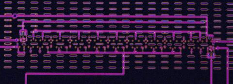
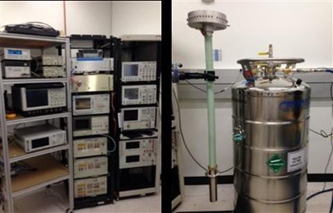
Fig. 8 shows some of the cryogenic test equipment that we developed during the C3 program and that we are using on the SuperTools program to test performer and NIST circuits.
Major Accomplishments
M. A. Castellanos-Beltran, D. I. Olaya, A. J. Sirois, C A Donnelly, P.D. Dresselhaus, S. P. Benz, and P. F. Hopkins, “Single-Flux-Quantum Multiplier Circuits for Synthesizing Gigahertz Waveforms with Quantum-Based Accuracy,” IEEE Trans. Appl. Supercond., vol. 31, 1400109, 3 Feb 2021, doi: 10.1109/TASC.2021.3057013.
A. J. Sirois, M. A. Castellanos-Beltran, A. E. Fox, S. P. Benz, and P. F. Hopkins, “Josephson Microwave Sources Applied to Quantum Information Systems,” IEEE Trans. Quant. Eng., vol. 1, 6002807, 18 Dec. 2020, doi: 10.1109/TQE.2020.3045682.
C. A. Donnelly, N. E. Flowers-Jacobs, J. A. Brevik, A. E. Fox, P. D. Dresselhaus, P. F. Hopkins, S. P. Benz, "1 GHz Waveform Synthesis With Josephson Junction Arrays," IEEE Trans. Appl. Supercond., vol. 30, 1400111, 3 April 2020, doi: 10.1109/TASC.2019.2932342.