
Official websites use .gov
A .gov website belongs to an official government organization in the United States.
Secure .gov websites use HTTPS
A lock (
) or https:// means you’ve safely connected to the .gov website. Share sensitive information only on official, secure websites.

The larger of the two alternating images above shows the topography of a nanowire bundle. The smaller image is the same bundle, but without the p-doped portion. The position of the p-n junction can be estimated from the difference.
NIST's ability to determine the composition and physics of nanoscale materials and devices is about to improve dramatically with the arrival of a new near-field scanning microwave microscope (NSMM).
The name may be a mouthful, but NSMMs deserve every syllable. Few techniques can make measurements of equivalent resolution for such a wide range of samples, including semiconductors, semiconducting nanowire, materials for photovoltaic applications, magnetic materials, multiferroic materials, and even proteins and DNA.
Researchers in PML's Electromagnetics Division, using existing commercial and home-made NSMMs, have pioneered many applications, notably including determination of semiconductor dopant distribution (i.e., charge-carrier concentrations) in 2D and 3D. That ability is required by a variety of emerging technologies, such as molecular electronics, carbon nanotubes, nanowires, graphene, and spin-based electronics. The new instrument is expected to accelerate that progress significantly.
"Basically, what we're doing is using the very fine spatial resolution of scanning probe instruments such as scanning tunneling microscopes or atomic force microscopes (AFM) and combining it with the broadband compatibility of microwave measurements," says Mitch Wallis of the Radio-Frequency Electronics Group. "Our motivation is that we want to look at things like magnetic resonance or mechanical resonance on the nanoscale using microwaves. If you look at your cell phone or your computer, they're all operating in the range of a few gigahertz. So we have to measure the nanoscale objects that make up those devices to get an understanding of how they perform at those frequencies. Otherwise, it's going to be much harder to integrate them into useful commercial devices."
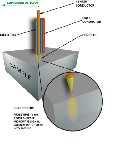
In broad outline, a NSMM set-up consists of an atomic force microscope combined with a continuous or pulsed microwave signal applied to the AFM tip. The tip scans across the sample in a soft contact or at a distance of a few nanometers above the surface, emitting a microwave signal that is scattered by the material, altering its frequency, amplitude and other properties. The nature of the altered signal returning to the tip – which also serves as the receiving antenna – depends critically on variables such as permeability, permittivity, sheet resistance, dielectric constant, impedance, or the manner in which capacitance changes with voltage, which in turn are determined by the physical composition of the object under investigation.
"By measuring the frequency-dependent scattered signal, we have, in effect, another knob to turn," says veteran researcher Pavel Kabos of the Advanced High-Frequency Devices Program. "And very recently we've been able to examine local properties of samples in extremely small dimensions, very close to the single-molecule level.
Spatial information recorded by the scanning tip is merged with data from the returning microwave signal at each point in a designated area (typically a few micrometers square) to create a composite image. NSMMs can be tuned to produce images at depths ranging from sub-micrometer to 100 μm below the surface. "So, for example, if you have a thin metal layer on top of the sample and a piezoelectric material underneath, you can see what's happening to the piezo material through the metal sheet," Kabos says.
It may seem counterintuitive that wavelengths on the order of a centimeter down to a few millimeters can provide nanometer-scale resolution. "It's something of a paradox," Kabos says, "until you look at the dimensions involved. The sharp AFM tip is only about 100 nanometers wide, and it is positioned only a few nanometers from the surface or is in a soft contact with the sample. It is the tip elevation that governs the resolution. The tip distance is so much smaller than the signal wavelength that 'near-field' effects predominate, permitting resolution in nanometers and highly accurate, quantitative measurements."
The researchers can alter both the tip voltage and the microwave frequency to examine different aspects of the sample. For example, in one 2012 paper, Atif Imtiaz and PML colleagues, along with researchers at instrument-maker Agilent Technologies, Inc., showed how changing the tip bias reveals the local carrier density in a semiconductor, and hence the dopant profile of a region. "Depending on the sign of the applied bias to the tip, the charge carriers in the semiconductor are attracted or depleted from the surface, forming a space charge region," the authors write.
Alternatively, changing the microwave frequency reveals other properties. "The same material may look very different at 5, 7, or 18 GHz," Kabos says. "So we can not only determine the doping profile locally, but also look at performance for a given frequency in a given region."
The new device, slated for a fall arrival, will provide many new capabilities. The existing instruments have a single tip that is open to the air. The new NSMM has four tips, permitting simultaneous comparisons of materials, and it is enclosed in an ultra-high vacuum chamber to minimize signal interference and sample contamination. It also features a vacuum sample-preparation chamber and temperature control from about 30 K to room temperature.
Among other uses, the new instrument will allow the researchers to explore in much greater detail the properties that affect the suitability of various materials, operating at microwave frequencies, for use in nanoscale electronics and bioelectronics, as well as emerging technologies for spintronic or phasetronic applications in single- and multi-layer configurations.
Future research will address several important areas. One is the possible development of reference materials. That effort will entail the creation of reliable, quantitative models for estimating local properties of materials and devices. Another area involves comparing and analyzing changes resulting from different variables, combining both voltage-dependent and frequency-dependent spectroscopy. There is considerable interest, for example, in measuring the derivative of the phase between incident and the reflected signal from the tip-to-sample load, as well as the currently measured derivative of capacitance as a function of voltage. That work could provide significant enhancements to the signal-to-noise ratio, improving sensitivity to water concentrations in biological samples and potentially enabling imaging of living biological cells in saline solution. Finally, there are plans to devise two-probe and multi-probe NSMM configurations that can measure complex microwave multi-port scattering matrix elements for broadband transport studies of systems such as high-frequency spintronics and carbon-based nanoelectronics.