
Official websites use .gov
A .gov website belongs to an official government organization in the United States.
Secure .gov websites use HTTPS
A lock (
) or https:// means you’ve safely connected to the .gov website. Share sensitive information only on official, secure websites.
Advanced Analytical Electron Tomography for Materials Development and Failure Analysis in Semiconductor Devices
Summary
Transmission electron microscopy (TEM) and scanning transmission electron microscopy (STEM) are widely used in industry for identifying structural and morphological characteristics in process development, control, and failure analysis. Existing TEM and STEM imaging methods struggle with complex semiconductor device architectures.
This project will develop quantitative, atomic-resolution methods for the three-dimensional characterization of complex semiconductor devices via electron tomography.
Grand Challenge 2. Advanced Metrology for Future Microelectronics Manufacturing
Description
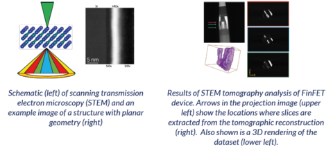
Conventional TEM imaging was sufficient for decades in the semiconductor industry, but its utility is declining as device designs become more complex and as feature sizes continue to shrink. Conventional imaging modes are challenged by the small, complex structures which are vital to current and developing technologies where it is not uncommon to find extreme variability in orientation, mass, crystallinity, and structure among nanoscale features that are in intimate contact with each other. A measurement method is needed that can characterize near atomic scale variability in device features such as roughness, thickness, length, and the presence and characteristics of defects in real world devices.
This project will deliver a robust suite of measurement tools to the semiconductor industry and address multiple CHIPS grand challenges in the process.
To advance semiconductor imaging capabilities, this project will:
- Enhance electron tomography's spatial resolution and accuracy for semiconductor industry needs.
- Leverage advancements in microscope resolution, detector sensitivity, and AI-based methods.
- Integrate AI for noise reduction, optimal data collection, and real-time reconstruction.
- Apply cutting-edge AI architectures like convolutional neural networks to improve fidelity and dose efficiency.
Success of this project will result in new measurement methods for immediate use by the semiconductor industry for addressing already existent problems as well as those which will arise in future technological processes as miniaturization and complexity continue to advance. The result will be a complete suite of methods for data acquisition, processing, and real-time reconstruction.