Taking Measure
Just a Standard Blog

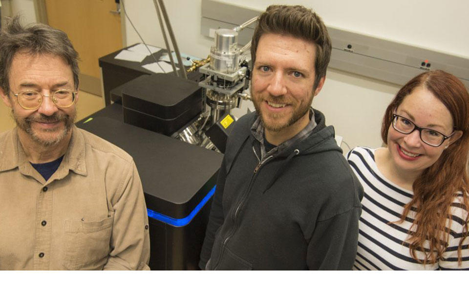
The APT team: Norman Sanford, Paul Blanchard (that's me!), and Ann Chiaramonti Debay.
Cars, buildings, computer chips, you and me and the air we breathe, everything is made of atoms. We learn this in elementary school, because, well, it’s an elementary fact. But we seldom think about it because we are big, and atoms are small—so small that, even with the help of the most powerful of microscopes, they’re almost completely invisible to us.
For most of our history, we humans have been pretty much clueless as to what’s going on at the scale of individual atoms. Despite our ignorance of this microscopic world, we’ve made some miraculous innovations just by studying the behavior of materials at the macroscopic scale. After all, we didn’t need to know anything about atoms to build pyramids or railroads or suspension bridges or skyscrapers or light bulbs. We didn’t even need to know anything about atoms in order to create entirely new materials like steel and plastic and fiberglass. We’ve proven to be pretty great at engineering even though the fundamental atomic composition beneath our designs has been shrouded in mystery.
But here’s the thing: With an understanding of that fundamental atomic composition, we can do even better.
Up to now, our technological progress has largely been a matter of trial and error. We make something new, evaluate its performance, then alter some part of the fabrication process and see whether it performs better or worse, all without direct knowledge of what is changing at the atomic level. But if we could see what’s going on at that scale—if we could map out each individual atom and understand the role that it plays—we could create new and better materials not through blind experimentation, but through design.

For all that we’ve been able to accomplish while ignoring them, the fact is that individual atoms matter. The speed of a transistor, the efficiency of a solar cell, and the strength of an I-beam are ultimately determined by the configuration of the atoms inside. Today, new and improved microscopy techniques are getting us closer and closer to the goal of being able to see each and every atom within the materials we make—a very exciting prospect.
Over the past three years, I’ve been lucky enough to be part of a team working with one such new and improved microscopy technique, a method called 3-D atom probe tomography, or APT for short. APT is very different from conventional microscopy—at least, the sort of microscopy that I’m accustomed to. In conventional microscopy, we shine a beam of light particles or electrons on our specimen, whatever it is we want to look at, and create a magnified image using lenses or by mapping how our beam bounces off it.
In atom probe tomography, on the other hand, we don’t just look at our specimen—we literally take it apart, atom-by-atom.

As we go along, a position-sensitive detector plate catches the ionized atoms that fly off the specimen, and we identify them using a mass spectrometer. The result is pretty amazing: a 3-D computerized rendering of the original specimen where each atom is identified as a particular element and placed in its original position. Considering how hard it is to do even two-dimensional microscopy at the atomic scale (let alone 3-D), APT seems almost like magic. But it’s even better than magic—it’s science!
Today, my colleagues at NIST and I use APT to study a wide variety of material systems. We’ve investigated superconducting films, LEDs, and laser-welded steel, among other things. APT allows us to provide valuable feedback to those who are developing all sorts of next-generation technologies by giving unprecedented insight into their atomic composition.
So have we reached the promised land of universal atomic-scale imaging? Not quite yet.
Powerful though it may be, APT is still relatively new. And like any new technology, APT is in many ways a work in progress. In fact, as we apply APT to different materials, we are learning as much about the capabilities and shortcomings of the technique itself as we are about the particular materials under study.
And we’ve found many opportunities for improvement. For one thing, we can only examine samples of minuscule size. And even within each small sample, we lose many atoms simply due to detector inefficiency. In addition, the atom-by-atom decomposition process is not always orderly and controlled—sometimes the atoms stick together to form small molecules, or multiple atoms hit the detector simultaneously. Issues like these can greatly complicate the interpretation of APT data. As a result, it takes a tremendous amount of careful experimentation and data analysis to achieve APT results that tell us something meaningful about the material.
But these challenges are exactly what make it such an exciting time to be working in the field of atomic-scale microscopy. At NIST, we get to help push the fundamental limits of measurement techniques like microscopy and contribute to the refinement of the new methods like APT. As we continue to improve APT and complementary techniques, such as transmission electron microscopy, we’re finally approaching a truly fine-grained knowledge of the materials we create. And since everything is made of atoms, these new capabilities will help to accelerate the development of all manner of next-generation technology, from lighter and stronger structures, to faster and more efficient electronics, to exciting new inventions that have yet to be realized.
That sounds to me like a very bright future indeed.
About the author
Related posts
Comments
- Reply


