Semiconductors
Strain Measurement for Semiconductor Devices and Packages
Mechanical strain impacts the performance of semiconductor devices. Manufacturing processes must be carefully controlled for strain to achieve high-yield and high-performance products. However, measuring strain in nanoscale devices remains a metrology challenge for manufacturers. This project will advance techniques to measure strain, advance techniques, improve accuracy, and supply new reference materials to ensure capabilities for future-generation devices.
Multiscale Modeling and Validation of Semiconductor Materials and Devices

A comprehensive understanding of how current and next-generation materials impact the performance of semiconductor devices is critical to U.S. semiconductor manufacturing. This project will develop qualitative and quantitative models for advanced semiconductor heterostructures, including material properties and the impact of the interface quality via multi-scale, multi-fidelity computational approaches.
Advanced Analytical Electron Tomography for Materials Development and Failure Analysis in Semiconductor Devices
This project will develop quantitative, atomic-resolution methods for the three-dimensional characterization of complex semiconductor devices via electron tomography. Transmission electron microscopy (TEM) and scanning transmission electron microscopy (STEM) are widely used in industry for identifying structural and morphological characteristics in process development, control, and failure analysis. Existing TEM and STEM imaging methods struggle with complex semiconductor device architectures.
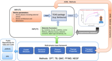
Ab Initio Theoretical Modeling for Predicting Structure and Properties in Advanced Materials

We develop first-principles-based methods for prediction of atomic arrangements and properties in advanced materials and develop tools for the prediction and interpretation of experimental x-ray absorption spectra, microscopy images, etc.

