Summary
One of the major obstacles to incorporating nanotechnology into everyday products is the difficulty of making nanoscale structures inexpensively over large areas. Advances in this area could affect the manufacture of everything from computer chips to solar cells. Block copolymers offer one route to addressing this problem, because they have an intrinsic nanometer length scale built in. The goal of this project is to develop new techniques to control and characterize the behavior of diblock copolymers for use in integrated circuit and data storage applications.
Description

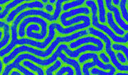
Diblock copolymers are long molecular chain polymers with two (di) regions, or blocks, of dissimilar monomers. They are constructed by covalently linking two different polymer chains at their ends. The two regions can be chosen so that they repel each other. Normally mixtures of different polymers tend to separate into large, single phase regions; but in a diblock, the covalent links between the chains prevent this from happening. The result is phase separation on the nanoscale, where the size of the different domains is controlled by the size of the two polymer molecules. Thin films of block copolymers are a simple, inexpensive route for large area patterning of nanoscale features because they can easily be coated onto a surface from a solvent solution. These systems can be converted to nanoscale masks for etching or deposition by preferential removal of one type of domain using relatively simple chemistry.
Typically, the domains do not form an ordered structure. However, by introducing a nanoscale chemical pattern on a surface, the diblock material can be made to order precisely over long distances. More importantly, the guiding pattern can be sparse and relatively imperfect. As a result, this technique has been suggested as a means to reduce feature size variation in integrated circuit fabrication, because the repulsion between the dissimilar blocks forces the block junction to a narrow interface.
However, for such a process to be used in computer chip manufacture, it must effectively be perfect: tiny variations in transistor dimensions adversely affect the overall performance of a chip. We are taking advantage of recent advances in low-energy x-ray diffraction methods to measure how the structure of the interface between block copolymer domains (i.e., chemical diffuseness) is linked to feature size variations. Diblock samples are aligned on ultra-thin (100 nm) silicon nitride membranes using nanoscale chemical patterns generated by electron-beam lithography. These aligned features then act as a diffraction grating for the x-rays. The deviations in the diffracted intensity from the ideal provide information on the average domain shape and edge-roughness.
Our approach can be used to observe changes in the domain structure dynamically to enable the optimization of a manufacturing process. It can also be applied to other important problems such as measuring the structure of interfaces in organic solar cells.
Selected Publication:
Measuring the structure of epitaxially assembled block copolymer domains with soft X-ray diffraction, G. E. Stein, J. A. Liddle, A. L. Aquila, and E. M. Gullikson, Macromolecules 43, 433-441 (2010).
NIST Publication Database Journal Web Site

