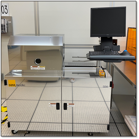
NanoFab Tool: Suss MicroTec SB6 Gen 2 Wafer Bonder

The Suss MicroTec SB6 Gen2 wafer bonder is a substrate bonder that’s equipped to handle a wide range of substrate bonding processes. The bonder accommodates standard size, semi spec wafers up to 150 mm in diameter and various shapes, and types of materials. Prior to bonding, substrate stacks can be mechanically clamped using a transport fixture. The transport fixture also fits into the Suss MA6 mask aligner, allowing users to pre-align their substrates before bonding.
Specifications/Capabilities
- Minimum chamber vacuum: 5 × 10⁻⁵ bar.
- Maximum temperature: 550 °C.
- Maximum bonding force: 20 kN.
- Power supply for anodic bonding: 2000 V, 60 mA.
- Substrate sizes: pieces to 150 mm.
- Maximum thickness: 9.99 mm.
Usage Information
Supported Sample Sizes
- Maximum wafer diameter: 150 mm.
- Small pieces supported: Yes.
Typical Applications
- MENS/NEMS devices.
- 3D photonic devices.
- Device packaging
- Thin film material transfer.
Created May 15, 2024, Updated March 4, 2025

