Materials Structure
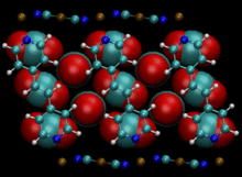
Ab Initio Theoretical Modeling for Predicting Structure and Properties in Advanced Materials

We develop first-principles-based methods for prediction of atomic arrangements and properties in advanced materials and develop tools for the prediction and interpretation of experimental x-ray absorption spectra, microscopy images, etc.
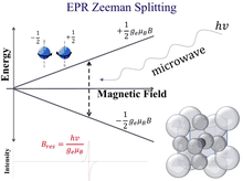
Measurements of Point-Defect Chemistry in Complex Oxides

Project Goal: To develop magnetic resonance, x-ray absorption, electron diffraction, and electrical conductivity measurements to better characterize dilute concentrations of point defects in oxide materials and effectively correlate electro-mechanical properties to measured defect chemistry.
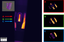
Sub-Nanoscale Electron Microscopy of Complex Nanostructures

The aim of this project is to develop robust, quantitative measurement methods utilizing transmission electron microscopy methods for complex, nanostructured devices with nanometer and sub-nanometer spatial resolution.
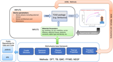
Multiscale Modeling and Validation of Semiconductor Materials and Devices

A comprehensive understanding of how current and next-generation materials impact the performance of semiconductor devices is critical to U.S. Semiconductor Manufacturing. This project will develop qualitative and quantitative models for advanced semiconductor heterostructures, including material properties and the impact of the interface quality via multi-scale, multi-fidelity computational approaches.
Measurement and Prediction of Local Structure

Our goal is to provide analytical tools that allow measurement and prediction of local structure to enable the development of ceramic materials for electronic applications. Under this project, we develop data analysis methods for quantitative determination of local structure from multiple experimental techniques, and theoretical methods for prediction of local atomic configurations from first principles.

