Measuring Up: Coming Out from the Cold
Novel design greatly improves output from commercial circuit boards next to superconducting qubits

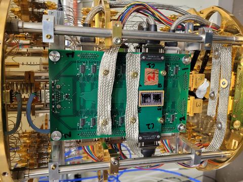
The photo shows green commercial circuit boards – the largest is 11.4 cm (4.5 in) by 19 cm (7.5 in) – inside a dilution refrigerator. When enclosed and pumped down, the system reaches temperatures only a few thousandths of a degree above absolute zero.
Researchers at the National Institute of Standards and Technology (NIST) have constructed and tested a system that allows commercial electronic components – such as microprocessors on circuit boards – to operate in close proximity with ultra-cold devices employed in quantum information processing. That design allows four times as much data to be output for the same number of connected wires.
In the rising excitement about quantum computing, it can be easy to overlook the physical fact that the data produced by manipulation of quantum bits (qubits) at cryogenic temperatures a few thousandths of a degree above absolute zero still has to be initiated, read out, and stored using conventional electronics, which presently work only at room temperature, several meters away from the qubits. This separation has obstructed development of quantum computing devices that outperform their classical counterparts.
That extra distance between the quantum computing elements and the external electronics requires extra time for signals to travel, which also causes signals to degrade. In addition, each (comparatively very hot) wire needed to connect the electronics to the cryogenic components adds heat, making it hard to maintain the ultracold temperature required for the quantum devices to work.
“If you consider our modern computers, what practically limits their speed is the time it takes information to move around between the CPU and graphics and memory – the physical distances, even though it is moving at the speed of light!” said the project scientist, Joshua Pomeroy. “Those finite distances kill the performance speed. Everything has to be as close as possible so the information gets there fast. So, you need electronics that live with the qubits.”
One obvious way to do that is to place the electronics package inside the cryo environment next to the quantum components. But until now, very few conventional circuit components have been shown to operate properly there. “Moreover, nobody really knows how much energy modern electronics consumes at these temperatures, which is another aspect in addition to just ‘getting something to work’,” Pomeroy said.
To expand circuit functionality at cryogenic temperatures, Pomeroy selected promising standard, commercial electronic chips and constructed a circuit designed to address another problem: the long time required to cool quantum devices, and the restricted number of measurement wires, bottlenecks how many devices can be measured. Since only one device at a time is measured, the new cryo-circuit routes each measurement line to a selected quantum device, “like a railroad switch yard where the track to a distant destination can be connected to many different local destinations, called multiplexing,” Pomeroy said. “In our case, we have 24 measurement lines, each of which can be connected to four different destinations. That requires a lot of switches.”
And all of those switches need to be set correctly. “We need to be able to control the switches (where the train goes) so that we choose which device on the cryo-stage is connected to each of the 24 wires that come out to room temperature,” Pomeroy said. For that task, he employed a standard device from room-temperature electronics: a “shift register” that uses only three control lines but can generate an arbitrarily complex set of control instructions.
“This device uses digital pulses (0 or 1) on the first measurement line that are timed by ‘clock’ pulses from a second wire to build a digital number – for example, 0010 – that selects the destination,” Pomeroy said. “In this example, the ‘1’ in the third position would route the measurement to the third device for measurement.” Once the address is set, a pulse on a third control line applies the selected address to the switches, and the measurements can begin.
The system quadruples the amount of measurement data that can be output without adding more wires.
“This work represents a milestone of technical effort that is important for enabling advanced measurement and technology at cryogenic temperatures,” said David Gundlach, chief of NIST’s Nanoscale Device Characterization Division.
“As one additional note,” Pomeroy said, “this entire effort took place during the pandemic shutdown at NIST Gaithersburg. My first (virtual) meeting with our electronics shop staff was in May 2020, and the planning and design continued through winter 2020. Parts and the custom devices were ordered in December and January, with final assembly and bench testing in the spring of 2021. The circuit boards were deployed for mounting and samples for testing in early summer. Since then, they have enabled more than 20 vastly different devices to be measured.”

