Using sugar and corn syrup (i.e., candy), researcher Gary Zabow transferred the word "NIST" onto a human hair in gold letters, shown in false color in this grayscale microscope image.
NIST scientist Gary Zabow had never intended to use candy in his lab. It was only as a last resort that he had even tried burying microscopic magnetic dots in hardened chunks of sugar — hard candy, basically — and sending these sweet packages to colleagues in a biomedical lab. The sugar dissolves easily in water, freeing the magnetic dots for their studies without leaving any harmful plastics or chemicals behind.
By chance, Zabow had left one of these sugar pieces, embedded with arrays of micromagnetic dots, in a beaker, and it did what sugar does with time and heat — it melted, coating the bottom of the beaker in a gooey mess.
“No problem,” he thought. He would just dissolve away the sugar, as normal. Except this time when he rinsed out the beaker, the microdots were gone. But they weren’t really missing; instead of releasing into the water, they had been transferred onto the bottom of the glass where they were casting a rainbow reflection.
“It was those rainbow colors that really surprised me,” Zabow recalls. The colors indicated that the arrays of microdots had retained their unique pattern.
This sweet mess gave him an idea. Could regular table sugar be used to bring the power of microchips to new and unconventional surfaces? Zabow’s findings on this potential transfer printing process were published in Science in its Nov. 25 issue.
Semiconductor chips, micropatterned surfaces, and electronics all rely on microprinting, the process of putting precise but minuscule patterns millionths to billionths of a meter wide onto surfaces to give them new properties. Traditionally, these tiny mazes of metals and other materials are printed on flat wafers of silicon. But as the possibilities for semiconductor chips and smart materials expand, these intricate, tiny patterns need to be printed on new, unconventional, non-flat surfaces.
Directly printing these patterns on such surfaces is tricky, so scientists transfer prints. There are flexible tapes and plastics that can do the job (like using putty to pick up newsprint), but these solids can still have trouble conforming to sharp curves and corners when the print is laid back down. They could also leave behind plastics or other chemicals that could be hard to remove or be unsafe for biomedical uses.
There are liquid techniques, where the transfer material is floated on the surface of water and the target surface is pushed through it. But that can be tricky too; with a freely flowing liquid it can be hard to place the print precisely where you want it on a new surface.
But, as Zabow discovered to his surprise, a simple combination of caramelized sugar and corn syrup can do the trick.
When dissolved in a small amount of water, this sugar mixture can be poured over micropatterns on a flat surface. Once the water evaporates, the candy hardens and can be lifted away with the pattern embedded. The candy with the print is then placed over the new surface and melted. The sugar/corn syrup combination maintains a high viscosity as it melts, letting the pattern maintain its arrangement as it flows over curves and edges. Then, using water, the sugar can be washed away, leaving just the pattern behind.
Using this technique, called REFLEX (REflow-driven FLExible Xfer), microcircuit patterns could be transferred like a stencil to allow scientists or manufacturers to etch and fill the materials they need in the right places. Or, patterned materials could be transferred from their original chip onto fibers or microbeads for potential biomedical or microrobotics studies, or over sharp or curved surfaces within new devices.
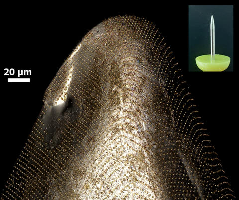
The technique proved successful for a large range of surfaces, including printing onto the sharp point of a pin, and writing the word “NIST” in microscale gold lettering onto a single strand of human hair. In another example, 1-micrometer-diameter magnetic disks were successfully transferred onto a floss fiber of a milkweed seed. In the presence of a magnet, the magnetically printed fiber reacted, showing the transfer had worked.
There’s still more to explore with REFLEX, but this process could open new possibilities for new materials and microstructures across fields from electronics to optics to biomedical engineering.
“The semiconductor industry has spent billions of dollars perfecting the printing techniques to create chips we rely on,” Zabow says. “Wouldn’t it be nice if we could leverage some of those technologies, expanding the reach of those prints with something as simple and inexpensive as a piece of candy?”
Paper: G. Zabow. Reflow transfer for conformal three-dimensional microprinting. Science. Published online Nov. 24, 2022. DOI: 10.1126/science.add7023


