
Official websites use .gov
A .gov website belongs to an official government organization in the United States.
Secure .gov websites use HTTPS
A lock (
) or https:// means you’ve safely connected to the .gov website. Share sensitive information only on official, secure websites.
High-Speed Waveform Metrology Group
The NIST CTL High-Speed Waveform Metrology Group develops fundamental measurement and characterization techniques for the high-speed devices and components at the heart of modern communications equipment.
The High-Speed Waveform Metrology Group supports a broad range of communications and computing technologies with particular importance to CTL Next-Generation 5G Wireless and Fundamental Metrology for Communications, and Quantum program areas. This work facilitates the development of standards and metrology essential for ultrafast circuits and systems that will power future communications and computing networks. The group's efforts are organized into three primary projects: High-Frequency Electronics, Waveform Metrology, and Quantum Networking and Transduction.
Capabilities
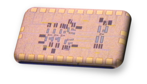
DC-THZ ON-WAFER MEASUREMENTS
This project is dedicated to improving the on-chip measurement of very-high-speed transistors (into the hundreds of gigahertz) as well as characterizing the nonlinear behavior of high-power, lower-frequency (microwave to millimeter-wave) transistors. Combinations of these transistors will be indispensable to next-generation wireless systems and open up a new high-frequency spectrum to the wireless industry. In addition to the High-Frequency Electronics Project, there are two exciting activities within this program sponsored by CHIPS and the NIST Innovations in Measurement Science awards: High-Frequency Transistor Modeling and “Getting from Qubit to Mega-Qubit Quantum Computers with RF Calibrations.”
PRIMARY WAVEFORM TRACEABILITY
This project has historically developed optoelectronic and statistical signal analysis techniques to characterize high-speed instrumentation used by the fiber optics, digital IC, and wireless industries as well as the Department of Defense (DoD) Primary Standards Laboratories and DoD contractors. Four NIST innovations lie at the core of the project’s work: calibration of impedance mismatch and loss effects in signal measurements; traceable electro-optic sampling (EOS) for frequency-response calibration; the calibration of timing errors, response errors, and impedance effects in sampling oscilloscopes; and uncertainty analysis that transforms waveform uncertainties between the time and frequency domains.
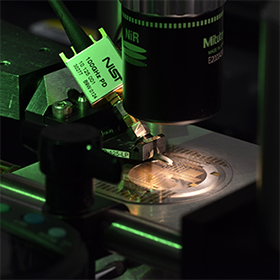
NIST was the first NMI to develop phase calibration capability through EOS and to map this calibration into waveform measurements and waveform measurement uncertainty. The Waveform Metrology Project maintains several calibration services that are used to provide traceability for commercial instrumentation, such as large-signal network analyzers, lightwave component analyzers, vector signal analyzers, oscilloscopes, pulsed laser radiometers, and optical time-domain radiometers. Recent efforts are working towards extending the EOS system to incorporate advanced techniques. One system spatially resolves waveforms by splitting the probe pulse image a number of points along a co-planar waveguide instantaneously. The dual comb system uses two optical frequency combs to independently control the pump and probe signals to increase the accuracy and speed of the measurement.
QUANTUM NETWORKING AND TRANSDUCTION
Efforts to increase the processing power of emerging superconducting quantum computers by simply adding more “qubit” circuit elements face daunting physical limits such as size, power, and circuit decoherence. The Quantum Networking and Transduction project is attempting to optically network individual processors to continue to scale them exponentially. The group's approach involves developing vibrating membrane quantum transducers which quantum mechanically connect the microwave processing domain with the optical transmission domain to establish remote microwave entanglement at the nodes of the network. This research effort involves the design and cleanroom micro-fabrication of the transducers, the generation and distribution of optical entanglement through optically squeezed states, and the cryogenic characterization and operation of the transducers in different schemes and topologies.
AWARDS
- 2022 - Allen V. Astin Measurement Science Award---Dazhen Gu, Aaron Hagerstrom, Benjamin Jamroz, Jeffrey Jargon, Christian Long, Ann F. Monke, Eric Stanfield, Angela Stelson, John Stoup, Dylan Williams | NIST For developing rigorous traceability with correlated uncertainties for microwave power and scattering parameters at 5G/6G communications frequencies.
- Jerome Cheron won the 2021 IEEE BiCMOS and Compound Semiconductor Integrated Circuits and Technology Symposium (BCICTS) Best Paper award for this work: https://www.nist.gov/news-events/news/2021/12/solid-state-thz-amplifier-breaking-records
Contacts
Group Leader (a)
-
(303) 497-5605