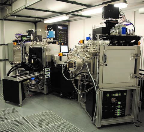
NanoFab Tool: 4Wave IBD/BTD Cluster Sputter Deposition System

The 4Wave IBD/BTD cluster sputter deposition system can automatically load and unload two six target chambers to provide users a largely unattended 24/7 deposition capability along with the densest available thin films via room temperature physical vapor deposition. An ion beam deposition chamber yields high density films that are pinhole-free and very smooth. A biased target deposition chamber allows adatom energy changes during film growth and minimizes interface mixing, while still depositing dense and very smooth films. The dual cassette load station supports substrates ranging from 200 mm diameter wafers down to small pieces.
Specifications/Capabilities
- Transfer robot and cassette elevators reduce contamination and allow fast cycle times.
- 24/7 unattended operation.
- Cryo-pumped process modules have a base vacuum of 2.6 x 10⁻⁶ Pa (2 x 10⁻⁸ Torr).
- Rotating stage for high uniformity deposition of thin films.
- Uniformity: 2 % (1 sigma).
- Stage temperature range: 20 °C.
- Quartz crystal thickness monitor.
- Residual gas analyzer.
- Ion guns for wafer pre-clean.
- Oxygen and nitrogen available for reactive sputtering.
- 12 fixed sputtering targets.
- List of available materials:
- Ag
- Al
- Al2O3
- Au
- Cr
- Co
- Co/Fe/B (72/18/10 wt %)
- Fe
- ITO
- Ni
- Ni/Fe (81/19 wt %)
- Pt
- SiO2
- Ta
- TaN
- Ti
- TiN
- TiO2
Usage Information
Supported Sample Sizes
- Maximum wafer diameter: 200 mm (8 in).
- Small pieces supported: Yes.
- Load capacity: 25 wafers
Typical Applications
- Electrical contacts.
- Dry etch masks.
- Magnetic materials.
- Electrical isolation.
Created January 15, 2015, Updated August 25, 2025

