Nanostructure Dimension Calibration

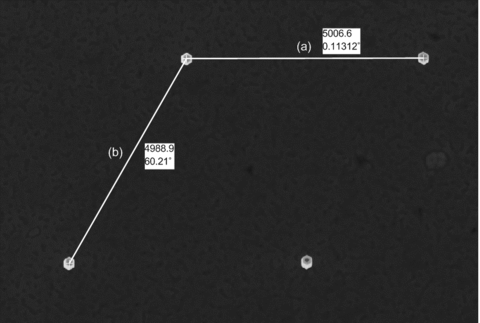
Fig. 1. Illustration of pitch measurement for tilt angle 0° using calibration factors of 9.875 nm/pixel and 9.885 nm/pixel, respectively, for x and y, as derived from SEM calibration for nominal magnification of 30,000. Only one of the ten measurements is illustrated for each line. See NIST SP250-96 for details of calibration procedures and uncertainty analysis. The pitch for line (a) is reported as 5000 nm ± 250 nm (k = 2), and the pitch for line (b) is reported as 5000 nm ± 200 nm (k = 2).
The accuracy of scanning electron microscopy (SEM) measurements depends on accurate calibration of the imaging process for each instrument. This Nanostructure Dimension Calibration provides traceable measurements of nanostructure diameter/width, height (measured with stage tilt) and pitch (lateral spacing relative to other nanostructures) for three-dimensional nanostructures. These measurements are traceable to NIST scanning electron microscope standards. One example of a pitch measurement is given in Figure 1. Details of the calibration process and recommendations for use as calibration standards in SEMs can be found in NIST Special Publication 250-96, available as a free download at https://doi.org/10.6028/NIST.SP.250-96. This special test is primarily intended for use with NIST Standard Reference Instrument 6012, which consists of precision semiconductor nanostructure arrays grown by molecular beam epitaxy (MBE) on a patterned substrate. Other calibration tests are possible by special arrangement. Please contact Kris Bertness (kris.bertness [at] nist.gov (kris[dot]bertness[at]nist[dot]gov)) for further information.
Resources
For quotes, scheduling, or shipping information:
John Lomax
Calibration Administrator
Physical Measurement Laboratory
325 Broadway
Boulder, CO 80305-3328
Tel: 303-497-3842
Fax: 303-497-4286
E-mail: john.lomax [at] nist.gov (john[dot]lomax[at]nist[dot]gov)
For technical information:
Kris Bertness
NIST Applied Physics Division
Tel: 303-497-5069
E-mail: kris.bertness [at] nist.gov (kris[dot]bertness[at]nist[dot]gov)
For information about other NIST calibration services:
Calibration Administrators
Physical Measurement Laboratory
E-mail: calibrations [at] nist.gov (calibrations[at]nist[dot]gov)

