Scanning Tunneling Microscope

|

|
|
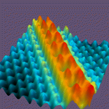
STM image, 7 nm x 7 nm, of a single zig-zag chain of Cs atoms (red) on the GaAs(110) surface (blue). Reference: Geometric and Electronic Properties of Cs Structures on III-V (110) Surfaces: From 1-D and 2-D Insulators to 3-D Metals, L.J. Whitman, J.A. Stroscio, R.A. Dragoset, and R.J. Celotta, Phys. Rev. Lett. 66, 1338 (1991). Electron Physics Group |
STM image, 35 nm x 35 nm, of single substitutional Cr impurities (small bumps) in the Fe(001) surface. Reference: Atomic-scale Observations of Alloying at the Cr-Fe(001) Interface, A. Davies, J.A. Stroscio, D.T. Pierce, and R.J. Celotta, Phys. Rev. Lett. 76, 4175 (1996). Electron Physics Group |
The scanning tunneling microscope (STM) is widely used in both industrial and fundamental research to obtain atomic-scale images of metal surfaces. It provides a three-dimensional profile of the surface which is very useful for characterizing surface roughness, observing surface defects, and determining the size and conformation of molecules and aggregates on the surface. Several other recently developed scanning microscopies also use the scanning technology developed for the STM. A precursor instrument, the topografiner, was invented by Russell Young and colleagues between 1965 and 1971 at the National Bureau of Standards (NBS) [currently the National Institute of Standards and Technology (NIST)].
Contents
For further information, contact: Bill Gadzuk (Gadzuk [at] nist.gov (Gadzuk[at]nist[dot]gov))
This exhibit was prepared by Marilyn E. Jacox of the Physics Laboratory and J. William Gadzuk of the Chemical Science and Technology Laboratory as a project of the NIST Museum Committee; both are currently in PML. It is one of the exhibit panels in the NIST Virtual Museum.
Exhibit layout designed by Gloria Wiersma and Bob Dragoset.
Online: November 1997

