
Official websites use .gov
A .gov website belongs to an official government organization in the United States.
Secure .gov websites use HTTPS
A lock (
) or https:// means you’ve safely connected to the .gov website. Share sensitive information only on official, secure websites.
Summary
Electronics manufacturers are always looking for transformative materials for future electronics. Two-dimensional (2D) and wide band gap (WBG) materials are some of the latest classes of materials with the potential to be transformative because of their high carrier mobilities, tunable bandgap, and atomic-scale film thicknesses.
This project will address a significant pitfall in electronics for national security that are based on wide-band gap materials and builds out a measurement framework for early adoption of next-generation electronics that contain 2D materials as functional components.
Grand Challenge 1: Metrology for Materials Purity, Properties, and Provenance
Description
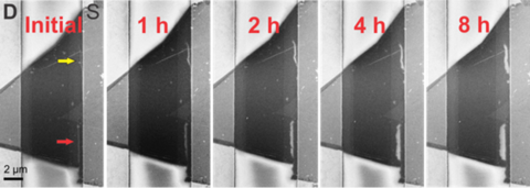
A time series of a MoS2 flake exposed to increasing time under electrical stress shows the growth of defects denoted with red and yellow areas over time. S= source and D = drain electrode.1
Two-dimensional (2D) and wide band gap (WBG) materials are some of the latest materials classes having the potential to be transformative because of their high carrier mobilities, tunable bandgap, and atomic-scale film thicknesses.
Unexpected degradation and failure in device performance is often traceable to poor material quality. Reliability is rooted in the stability of the atoms making up a material, and is determined by geometry, microstructure, chemistry, defect density, dimensional scale, proximity to other materials, and exposure to external stressors. Integration of powerful characterization techniques and reliability tests of materials under operational conditions improves fundamental understanding and accelerates development of high-quality reliable materials and devices.
NIST will work with US manufacturers to improve manufacturing processes of advanced material devices with the immediate goal of evaluating the feasibility of using 2D materials.
To date, manufacturers have emphasized product development with little to no attention given to device reliability issues. New advanced 2D materials are currently tested in an ad hoc manner by manufacturers, and most reliability test procedures for devices utilizing gallium nitride (GaN) are based on existing Complementary Metal-Oxide-Semiconductor (CMOS) protocols that don’t adequately address the application space of the material.
This project aims to support the industry by developing recommendations that can be implemented prior to commencing large-scale manufacturing efforts to enhance device reliability. NIST is well positioned to help address early reliability issues by employing and developing electrical, thermal, and mechanical stress test methods that enable electronic material and device manufacturers to predict how and when failures will occur and enable lifetime analyses appropriate for their desired performance level