FPGA-based Digital Control Box for Phase Stabilization of a Frequency Comb

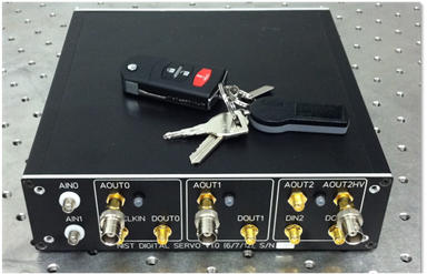
Figure 2. Photo of the digital control box.
This page provides information on firmware/software used at NIST to phase-lock a frequency comb. The firmware/software operates with hardware that was developed at NIST by David Leibrandt and is described in detail at https://github.com/nist-ionstorage/digital-servo.
The firmware/software allows the use of this hardware to phaselock a frequency comb. More generally, together with the hardware, it provides a digital control box that can support a dual-channel phase-locked loop including the front-end IQ detection of the input rf signals. While this digital control box could therefore be used to phase lock other systems, the discussion below assumes the user is operating a frequency comb.
In order to use this firmware/software, it is necessary to first construct the hardware, which includes a custom daughterboard. Therefore, the potential user is encouraged to first make sure this system is suitable for his or her needs by reading the information below and the instructions file.
Background:
Details on the NIST frequency comb system are provided in the Review of Scientific Instruments article. The information below is mainly extracted verbatim from that article.
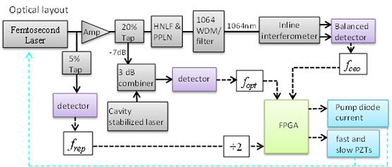
The overall frequency comb system is depicted in Figure 1.
The digital control box is shown in Figure 2. It follows directly the description at https://github.com/nist-ionstorage/digital-servo except that the daughter ADC board is modified by insertion of a jumper to allow high bandwidth (up to 50 MHz) operation as specified in FPGA Box High Bandpass Modification Schematic.pdf.
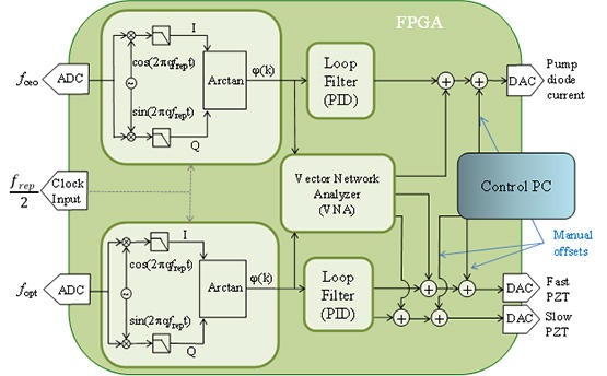
Figure 3 provides a basic outline of the FPGA-based control system, which consists of input analog-to-digital converters (ADCs), an in-phase and quadrature (IQ) detection module for detection of the phase, a loop filter, output DACs, and built-in real-time diagnostics through zero-deadtime frequency counters, phase-noise analyzers, and a vector network analyzer (VNA) for transfer function measurements. As mentioned, this is currently implemented with hardware originally designed by David Leibrandt for locking cw lasers to ultra-stable optical cavities and consists of a custom analog input/output daughterboard and an OpalKelly XEM integration module with Xilinx Spartan-6.
The two 16 bit, dc-coupled ADC inputs operate with a 50 MHz input bandwidth and 100 MS/s. One 16-bit DAC output is used for the pump diode current control and two 16-bit DACs are used for the PZT control, one of which (the "slow PZT output" in Fig. 3) is a 0-64 V output. The FPGA is clocked directly from half the repetition rate, enabling self-referenced operation. (The system can also be operated from an internal clock.) Standard digital-signal-processing routines are implemented, as described qualitatively below.
The RF signals fceo and fopt are digitized and mixed downvia IQ detection against the phase-lock frequency, q frep (which is in general different for the two phase locks). For a fully self-referenced system, this lock frequency, q frep, is derived from frep and q = M/N, where M is any integer and N = 248. The phase of the baseband signal is calculated using an arctangent operation and unwrapped (not shown in the diagram) to ±3 × 10⁶ radians of linear range, which allows linear behavior even under significant perturbations. As long as frequency/phase excursions caused by environmental perturbations to the frequency comb do not exceed the input filter bandwidth (25 MHz in this work), they are tracked and the phase is recovered without 2p ambiguities. The loop filter which follows the phase unwrapping operation is a tunable proportional integral/derivative (PID) filter.
A built-in VNA allows for measurement of transfer functions and real-time monitoring of residual lock phase noise. When desired, the VNA can provide a small dither to any of the output signals to measure the transfer function of any given modulator in the frequency comb or to measure the sign of optical or CEO beats (to determine if the cw laser above or below the comb tooth in the fopt signal, for example). During normal operation, the dither is off and the VNA passively monitors residual phase noise on the locks. The FPGA also has implemented two zero-deadtime, triangular averaging frequency counters operating at a 1-s gate time to monitor the long-term performance.
Firmware/Software:
In addition to the instruction manual and readme file. The main zip file includes
- Python code for the GUI interface with the digital control box. This code automatically loads the bit file onto the target FPGA.
- The bit file for the FPGA.
An additional zip file is available upon request that includes the VHDL code. This code is not supported by any additional documentation or current NIST programs. It is supplied as is.
Related Publications
Sample Screenshots

Figure 1: Overall frequency comb system. The digital control box is indicated by the green box labeled FPGA (except that the ÷2 on the clock signal is also integrated within the FPGA).

Figure 3. Block diagram of the FPGA operations.
Contact
-
(303) 497-5050
-
(303) 497-4889
-
Primary contact for firmware/software information:

