
Official websites use .gov
A .gov website belongs to an official government organization in the United States.
Secure .gov websites use HTTPS
A lock (
) or https:// means you’ve safely connected to the .gov website. Share sensitive information only on official, secure websites.
GlobalFoundries (New York)
Key Facts
Project Summary
The U.S. Department of Commerce awarded GlobalFoundries (GF) up to $1.587 billion in direct funding under the CHIPS and Science Act. The award will bolster U.S. competitiveness in current-generation semiconductor production by supporting the company’s capital investment of approximately $14 billion over the next 10-plus years in its U.S. manufacturing sites in New York and Vermont. The investment includes a new state-of-the-art facility in New York, the capability and capacity expansion of an existing facility in New York, and the modernization of the company’s operations in Vermont. The projects will create approximately 9,000 construction and 1,100 manufacturing jobs across both sites.
Economic and National Security Impact
This investment in GF will advance U.S. economic and national security by increasing domestic manufacturing capacity, strengthening supply chain resilience, and onshoring technologies in the U.S. for the first time that are important to the U.S. defense and intelligence communities. GF’s manufacturing sites in New York and Vermont produce essential automotive, communications, defense, and other semiconductor technologies.
The $1.575 billion in direct funding will be split across GF’s projects:
Malta, New York – New State-of-the-Art 300mm Fab: The construction of a new, large-scale 300mm fabrication facility that is expected to produce high value technologies not currently available in the United States. The new facility is intended to leverage existing infrastructure to expedite the path from construction to production.
- Malta, New York – Capacity Expansion for Advanced Packaging: The expansion of the existing campus to provide first-of-its-kind advanced packaging technology, with a focus on critical technologies such as silicon photonics. The expansion would enable a fully integrated pureplay foundry wafer manufacturing and advanced packaging process flow in the United States for the first time.
- Malta, New York – Capacity Expansion for Automotive: The expansion of GF’s existing Malta, New York, fabrication facility to secure a dedicated supply of essential semiconductor technologies.
Burlington, Vermont – Fab Revitalization: The revitalization of an existing fabrication facility in Burlington, Vermont, to commercialize new 200mm technologies, including Gallium Nitride on Silicon. The revitalization would create the first U.S. facility capable of high-volume manufacturing of next-generation Gallium Nitride on Silicon for use in electric vehicles, power grid, 5G and 6G smartphones, and other critical technologies.
Currently, there are only four companies outside of China that provide current and mature foundry capabilities at the scale of GF – and GF is the only one of those companies that is headquartered in the United States. Shortages of some of these semiconductors caused major disruptions during the COVID-19 pandemic, resulting in a particularly acute impact on the availability and price of a broad range of goods for Americans, as well as the shutdown of automobile manufacturing sites.
Financial and Commercial Terms
As stated in the CHIPS Notice of Funding Opportunity (NOFO) for Commercial Fabrication Facilities, the CHIPS Program Office (CPO) will disburse direct funding to GlobalFoundries for capital expenditures for the project based on the completion of construction, production, and commercial milestones. CPO will track the performance of each CHIPS Incentives Award via financial and programmatic reports, in accordance with the award terms and conditions. All CHIPS funding recipients are required to adhere to restrictions pursuant to the CHIPS Act and the NOFO regarding stock buybacks and National Security Guardrails. The Department and GF have agreed to certain conditions on buybacks for a period of 5 years.
Workforce, Community, and Environmental Commitments
As part of our commitment to transparency, for information on the local and community impact of this project, please download our Community Impact Report.
GlobalFoundries Project Overview | ||
|---|---|---|
Project Summary | Recipient | GlobalFoundries |
| Location(s) | Malta, New York Burlington, Vermont | |
Financial Summary | Program | CHIPS Program Office |
| Direct Funding Amount | $1.587 billion | |
| Expected Capital Expenditure | $14 billion | |
Workforce Summary | Estimated Job Creation | 1,100 manufacturing jobs and 9,000 construction jobs |
| CHIPS Workforce Funding | $12 million | |
Project Statistics: Malta, New York | ||
|---|---|---|
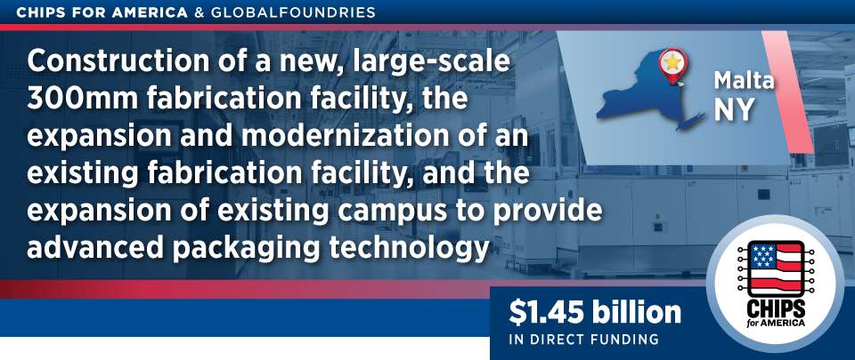
Summary | Project Type | Construction of a new, large-scale 300mm fabrication facility, the expansion and modernization of an existing fabrication facility, and the expansion of existing campus to provide advanced packaging technology |
| Technology | 300mm high value technologies for automotive and defense uses not currently available in the U.S. Advanced packaging technology focused on silicon photonics, chiplet integration and wafer-to-wafer bonding, supporting AI, high-performance compute, and communications end markets | |
| Estimated Job Creation | 1,100 manufacturing jobs 8,000 construction jobs | |
| Direct Funding | $1.45 billion | |
Related Links
- Press Release: U.S. Department of Commerce Announces CHIPS Incentives Awards with Corning, Edwards Vacuum, and Infinera to Increase Domestic Production Capacity of Chips and Equipment Critical for U.S. Technological Leadership
- Biden-Harris Administration Announces CHIPS Incentives Award with GlobalFoundries to Strengthen Essential Chip Supply for Key U.S. Industries Including Auto and Defense
- Biden-Harris Administration Announces Preliminary Terms with GlobalFoundries to Strengthen Domestic Legacy Chip Supply for U.S. Auto and Defense Industries
- GlobalFoundries Community Impact Report
- Fact Sheet: CHIPS Program Office Approach to Applicant Capital Allocation Policies
Site Photos


