
Official websites use .gov
A .gov website belongs to an official government organization in the United States.
Secure .gov websites use HTTPS
A lock (
) or https:// means you’ve safely connected to the .gov website. Share sensitive information only on official, secure websites.
Applied Materials
Key Facts
Purpose
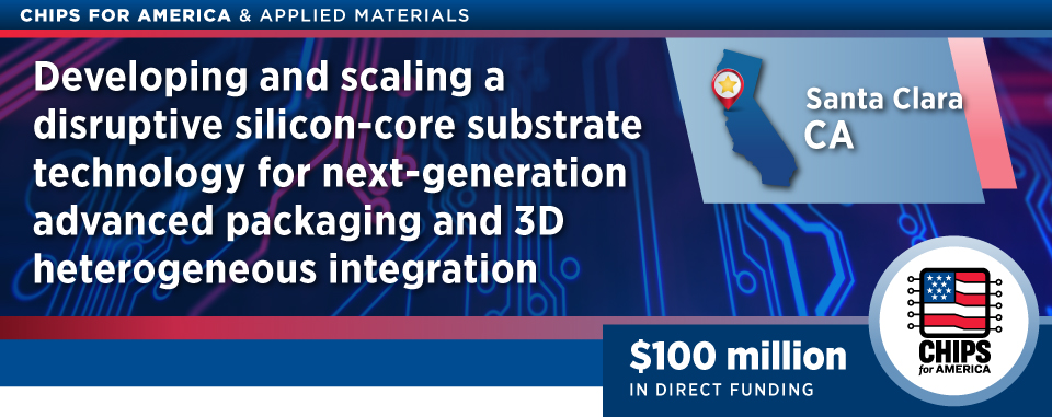
The U.S. Department of Commerce awarded Applied Materials, Inc. $100 million in direct funding to develop and scale a disruptive silicon-core substrate technology for next-generation advances in packaging and 3D heterogeneous integration. Key demonstrator technologies for advanced packaging will be validated through this program.
These advanced substrates are physical platforms that allow multiple semiconductor chips to be assembled seamlessly together, enable high-bandwidth communication between those chips, efficiently deliver power, and dissipate unwanted heat.
Expected Outcomes
Along with a team of 10 collaborators, Applied Materials silicon-core substrate technology has the potential to advance America’s leadership in advanced packaging and help catalyze an ecosystem to develop and build next-generation energy-efficient artificial intelligence (AI) and high-performance computing (HPC) systems in the US. Leadership for advanced 300mm silicon packaging substrates and materials will be achieved by meeting the aggressive targets set in this project. Silicon-core substrates will enhance key advanced packaging technologies, including but not limited to equipment, tools, processes, and process integration.
Workforce Development
Applied Materials will work with university partners to provide internships and graduate research opportunities for graduate, undergraduate, and training in community colleges for students in advanced packaging, chiplet integration in fabrication facilities, and chiplet/substrate design. Educational modules will be developed to support ASTM certifications across important microelectronic manufacturing processes.
About the CHIPS National Advanced Packaging Manufacturing Program (NAPMP)
To enable the CHIPS Research and Development Office’s vision for success, the CHIPS NAPMP will make approximately $3 billion in investments to develop critical and relevant innovations for advanced packaging technologies and accelerate their scaled transition to U.S. manufacturing entities. These investments will include research programs for core technologies that can be scaled to high-volume manufacturing, an advanced packaging piloting facility to support this scaling, resources to support the expansion of advanced packaging solutions, and workforce development. As a result, within a decade, NAPMP-funded activities, coupled with CHIPS manufacturing incentives, will establish a vibrant, self-sustaining, high-volume, domestic, advanced packaging industry where advanced-node chips manufactured in the United States are packaged in the United States. The technology developed will be leveraged in new applications and market sectors and at scale.
Financial Summary | Program | CHIPS NAPMP |
Direct Funding Amount | $100 million | |
Expected Co-Investment | $54 million |
Read the full CHIPS for America press release by clicking here.
Learn more about the CHIPS NAPMP by clicking here.