Summary
The goal of the BIB-Trap Detector project is to develop a detector composed of solid-state devices that can be used as a reference detector for calibrations in the wavelength range 4-28 µm. Blocked-impurity-band (BIB) devices with arsenic-doped silicon IR-active layers presently provide excellent noise performance in this wavelength range, but suffer from inhomogeneous spectral response and internal losses. In this project, novel BIB devices with minimal internal losses have been developed and will be combined in a trapping configuration to attain a flat spectral response and overall quantum efficiency greater than 98%.
Description
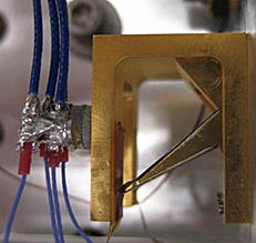
Prototype BIB-trap detector mounted in a cryostat.
Limitations of Standard BIB Detectors
Currently available BIB detectors exhibit excellent detectivity, but are limited in their use for spectral calibrations by detection inefficiency and spectral response inhomogeneity. The maximum quantum efficiency of these doped silicon devices is near 60%, mostly as a result of loss from reflection at the incident surface. Although this external loss could be recouped by arranging multiple such detectors in a trapping arrangement, there are also internal losses in standard BIBs which would limit the quantum efficiency of a trap detector constituted from them. For this reason, we have developed novel high internal efficiency BIBs for use in our trap detector.
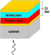
Internal losses in standard backside-illuminated BIBs are unavoidable because photons must pass through hundreds of micrometers of silicon substrate before reaching the IR-active layer. In addition, there can be absorption in the nominally transparent contact layer between the substrate and IR-active layer, as well as loss from transmission through the reflective back contact of the device. A limited amount of photon energy can pass through the device to the back contact, reflect back to the front surface and escape without absorption. Aside from internal losses, another problem is that the spectral response shows significant inhomogeneity in the form of oscillations and absorption features, as seen in part b of the figure below. The oscillations result from Fabry-Perot interference between the parallel layers of the detector, and the largest absorption features are from the silicon substrate.

New High Internal Efficiency BIB Devices
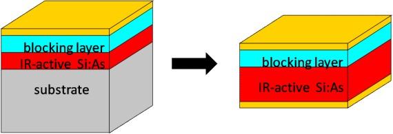
The novel BIB devices, developed with DRS Sensors and Targeting Systems, Inc., have two principal design features to maximize their internal efficiency and optimize trap detector performance. The first design feature is that the backside silicon of the devices is polished away after fabrication, as shown below, so that photons only pass through a thin transparent contact before reaching the IR-active layer. In this way, absorption losses in the substrate can be avoided. The second design feature is that the IR-active layer has been made significantly thicker than in standard BIBs. The greater thickness reduces potential loss through transmission at the back contact, and reduces the relative power that can be lost through photons which execute a round-trip through the device and escape back out the incident surface.
Trap Detector Design
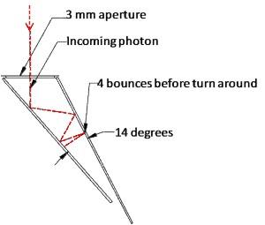
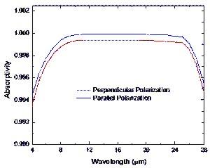
The geometry chosen for the trap detector is a wedge composed of two nominally identical BIB detectors. The schematic of the trapping arrangement is shown in part a of the figure below, and the modeled external quantum efficiency of such a trap is presented in part b. By design, incoming photons will execute a minimum of 7 bounces in the trap before escape. It has been estimated by the manufacturer that the new BIBs could achieve 99% internal quantum efficiency; assuming this performance, the BIB trap detector could achieve greater than 98% total quantum efficiency over the wavelength range 4-28 µm.
Major Accomplishments
- Modeled behavior of novel BIB designs
- Modeled behavior of trap detector geometries
- Designed and fabricated novel BIB detectors
- Designed and machined trap mount
- Assembled and tested prototype traps

