
Official websites use .gov
A .gov website belongs to an official government organization in the United States.
Secure .gov websites use HTTPS
A lock (
) or https:// means you’ve safely connected to the .gov website. Share sensitive information only on official, secure websites.
SRI 6012 Precision Semiconductor Nanostructures
Technical Contact: kris.bertness [at] nist.gov (Kris Bertness)
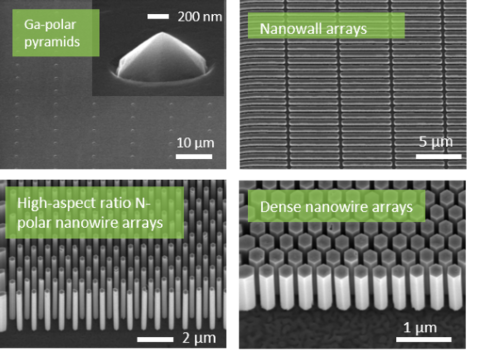
Precision semiconductor nanostructure arrays are grown by molecular beam epitaxy (MBE) on a prepatterned substrate. Following buffer layer deposition, the substrate is coated with a mask layer that allows selective regrowth in areas where the mask has been removed. Lithographic processing controls the placement and diameter of subsequent nanostructure regrowth. Measurements of three critical dimensions of specific nanostructures on the SRI are provided with traceability to NIST RM 8820, Scanning Electron Microscope Scale Artifact. Details of the calibration process with examples can be found in NIST Special Publication 250-96, available as a free download at https://doi.org/10.6028/NIST.SP.250-96. Fabrication methods for the precision nanostructures are based on those described in M. D. Brubaker, et al., Crystal Growth & Design 16, 596 -604 (2016), DOI: 10.1021/acs.cgd.5b00910.
Specifications Certificate (PDF Format) (attached)
To obtain a quote for the instrument and calibration services, please contact Sales and Customer Service by email at srminfo [at] nist.gov (srminfo[at]nist[dot]gov).
| 6012a | Nanostructure arrays on MBE-grown buffer | |
| 6012b | Nanostructure arrays without buffer | |
| 6012c | Nanostructure extended arrays on MBE-grown buffer | |
| 6012d | Nanostructure extended arrays without buffer |